What exactly is ESD, and why can it damage electronics before anyone realizes it happened?
Electrostatic discharge can cause immediate or latent damage to sensitive semiconductor and electronic components.
Our new guide explains how ESD happens, why it matters, and how protective packaging helps reduce the risk.
https://t.co/KM4q6hACTe
#ESD #SemiconductorPackaging
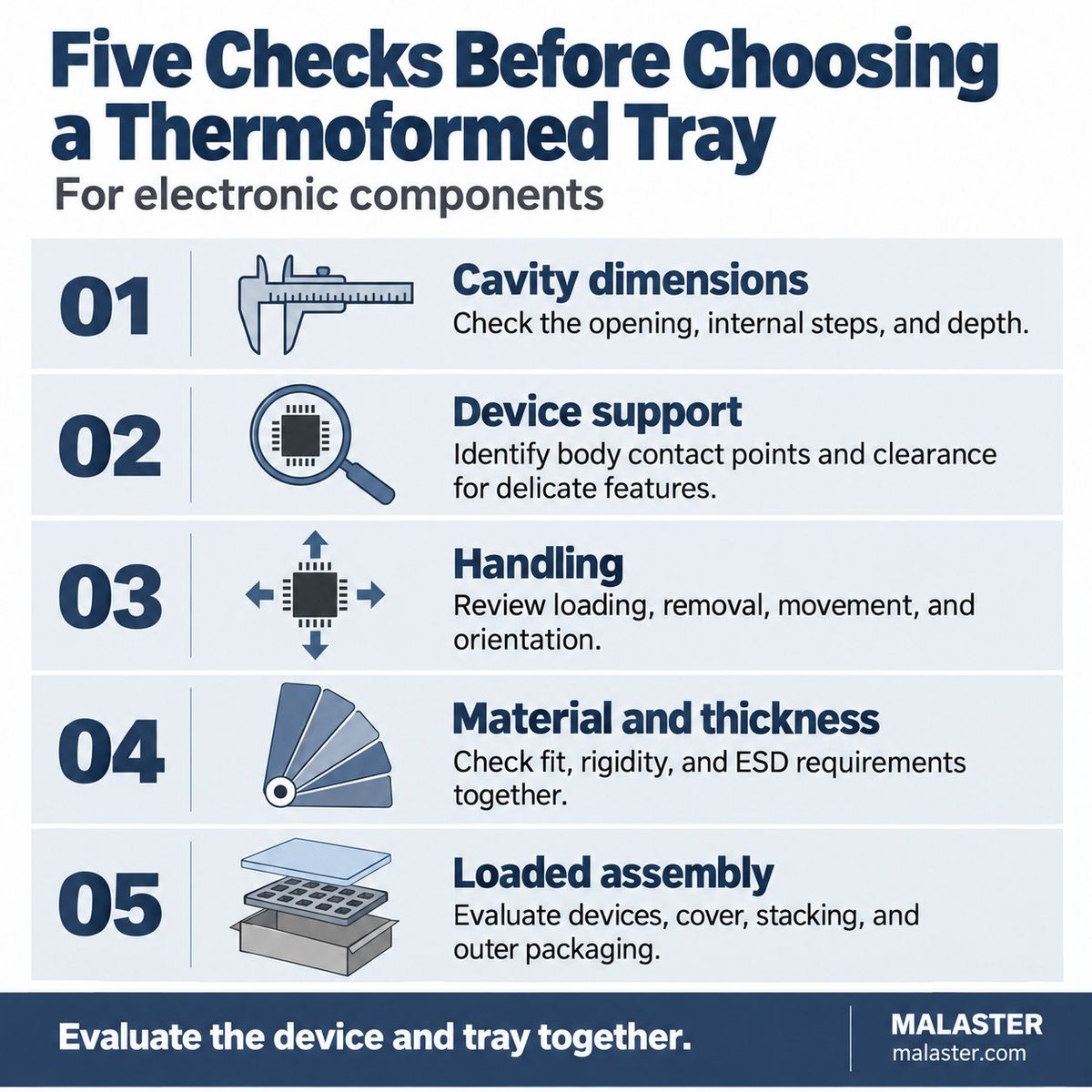
Fit is only the starting point. Check cavity dimensions, device support, handling, material, and the loaded assembly before choosing a thermoformed tray.
https://t.co/1hjecuwx8A
#SemiconductorPackaging
Twenty-five years later, we remember the lives lost on September 11, 2001, honor those who stepped forward to help, and keep the families, survivors, and first responders in our thoughts.
#September11#WeRemember
Gull-wing. Not bent-wing.
A static-shielding bag isn't a lead protector. Delicate SOIC leads need a fitted carrier, too.
Connections. Not bumpers.
https://t.co/90cLW8Pr4q
#ESD#Semiconductors
Before the tape goes on, check what is happening inside the package. Our new guide covers five practical checks for shipping loaded IC tubes and other electronic components.
https://t.co/Jtd5Fwfcc2
Small cutouts. Different jobs.
Side slots provide access for wafer placement and removal. Corner relief gives fragile wafer corners clearance.
See how foam, separators, and fit work together in wafer jar packaging:
https://t.co/VWvIpC910s
This Labor Day, we recognize the skilled people behind the equipment, processes, and attention to detail that make dependable protective packaging possible.
Wishing everyone a safe and well-earned holiday weekend.
#LaborDay#Manufacturing