SEMICON Europa 2025, here we come! 🇩🇪
We're looking forward to connecting with industry leaders and sharing our expertise.
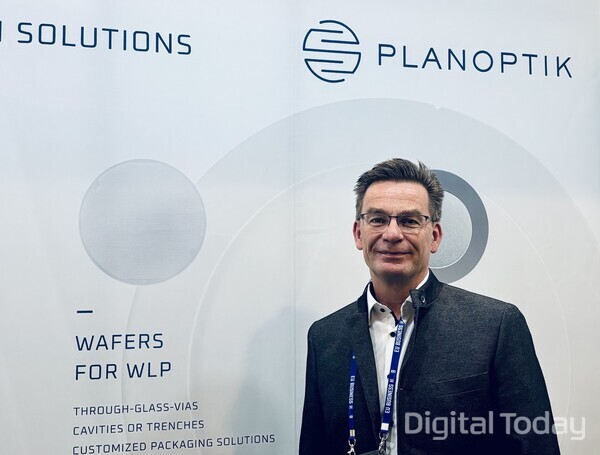
Find us at Booth B1912! Let's talk business.
#SEMICONEuropa#PLANOPTIKAG#Munich#Germany
Join us at Semicon Europa 2024 from November 12-15, 2024.
Come visit us at Booth #C1562 to discover our latest innovations and solutions!
Looking forward to meeting you there!🤝
#SemiconEuropa2024#PLANOPTIKAG#WaferUniverse
We are excited to announce that our team will be attending Semicon Europa 2024 from November 12-15, 2024.
Come visit us at Booth #C1562 to discover our latest innovations and solutions!
Looking forward to meeting you there!🤝
#SemiconEuropa2024#PLANOPTIKAG#WaferUniverse
We are excited to announce that our team will be attending Semicon Europa 2024 from November 12-15, 2024.
Come visit us at Booth #C1562 to discover our latest innovations and solutions!
Looking forward to meeting you there!🤝
#SemiconEuropa2024#PLANOPTIKAG#WaferUniverse
We're excited to announce that PLANOPTIK AG will be attending the 10th IEEE Electronics System-Integration Technology Conference in Berlin! Join us from September 11-13 to learn more about our latest innovations in electronics system integration.
#IEEEESTC2024#PLANOPTIKAG
We're excited to announce that PLANOPTIK AG will be attending the 10th IEEE Electronics System-Integration Technology Conference in Berlin! Join us from September 11-13 to learn more about our latest innovations in electronics system integration.
#IEEEESTC2024#PLANOPTIKAG
We're excited to be at Semicon Taiwan 2024 in Taipei! 🎉 Come visit us at our booth #N0566 we're here and ready to connect with you. Don't miss out on seeing our latest innovations. We look forward to meeting you! #SemiconTaiwan#PLANOPTIKAG#Waferuniverse
Plan Optik becomes PLANOPTIK
We have a new name. Plan Optik AG was renamed PLANOPTIK AG at the last Annual General Meeting. At the same time as the change of name, the PLANOPTIK Group is also getting a new logo.
Read more: https://t.co/iHODaHRJAg
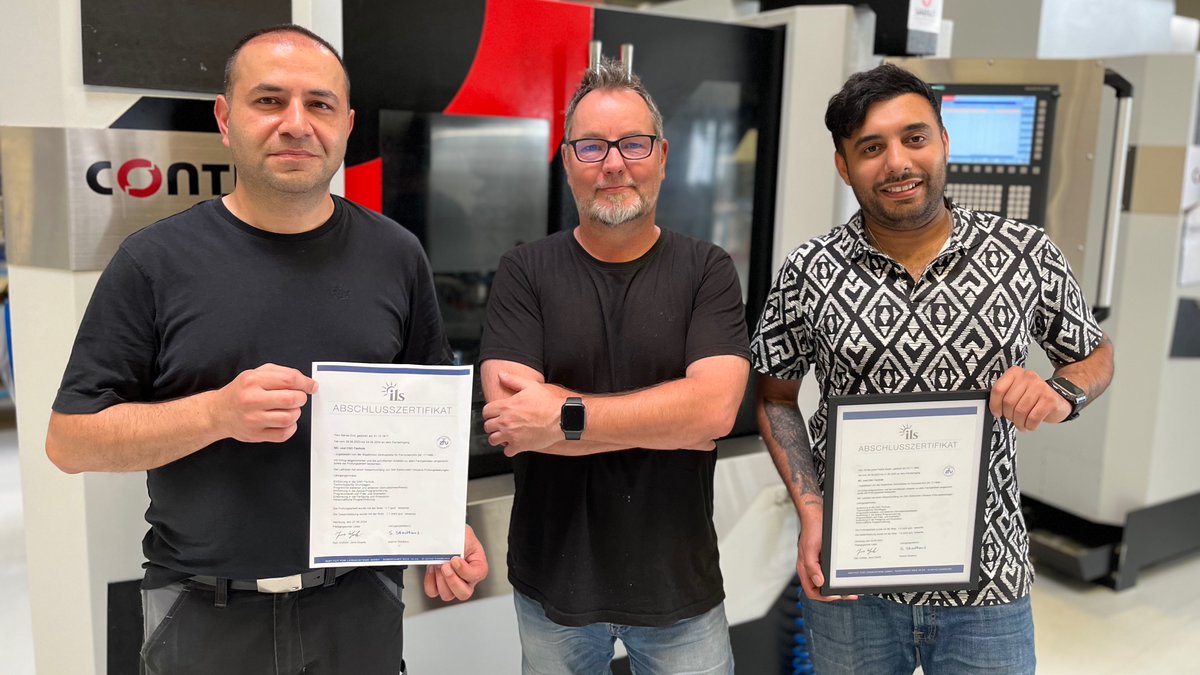
🎉 Herzlichen Glückwunsch an unsere Kollegen Erol Savas und Ali Alsabr! 🎉
Erol und Ali haben erfolgreich ihre Weiterbildung im Bereich NC- und CNC-Technik abgeschlossen.
#planoptik#karriere#weiterbildung#weareplantopik
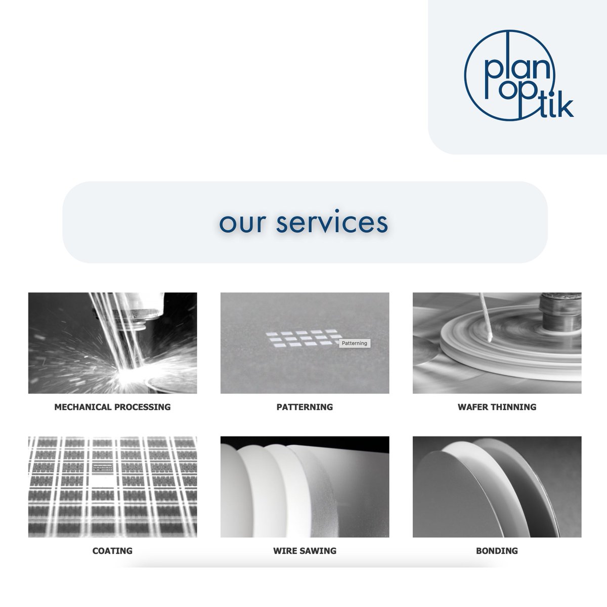
Pioneering Volume Laser Induced Structuring (VLIS) Technology
Plan Optik AG presents Volume Laser Induced Structuring (VLIS), a next-generation solution designed to meet the demands of cutting-edge semiconductor applications.
Read more: https://t.co/a2KSr9ZsVj
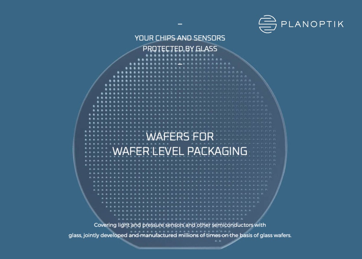
The growing importance of Glass Substrates in Semiconductor Technology
The semiconductor industry is experiencing a significant shift towards the use of glass substrates, driven by their superior performance characteristics and suitability ... Read more: https://t.co/ZMHzkhKFhj
We’re excited to be part of Sensors Converge 2024!
Join us from June 24-26, 2024, at the Santa Clara Convention Center in Santa Clara, CA.
You can find us at booth #409.
#sensorsconverge#santaclara#planoptikag#waferuniverse
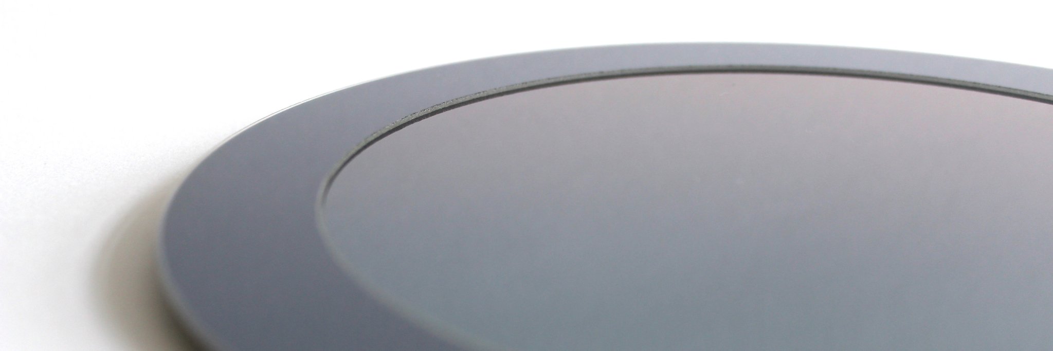
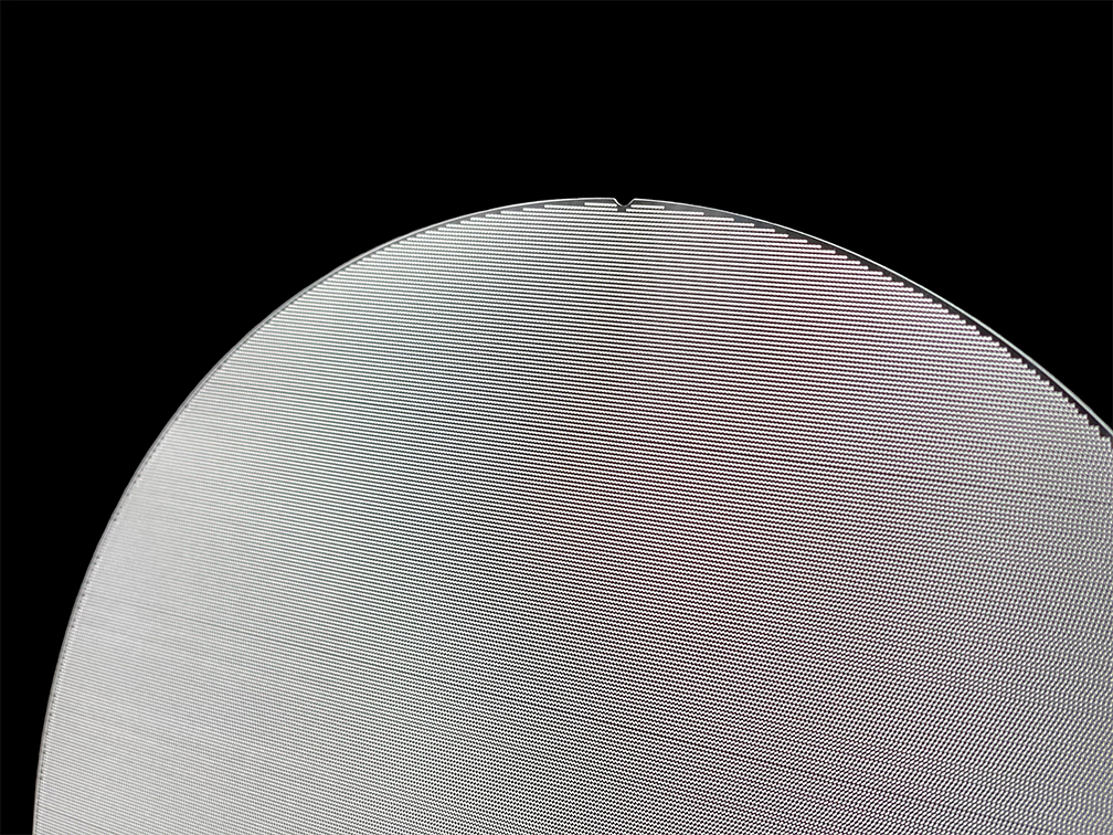
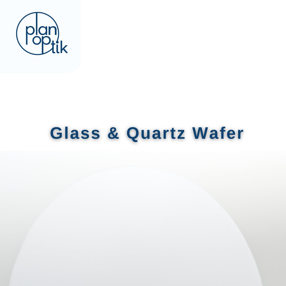
Plan Optik manufactures wafers for wafer level packaging from various types of glass, quartz, alkaline free glass and glass-silicon compound materials.
more: https://t.co/DklLU7kvDb
Welcome to the wide range of customized glass wafer from Plan Optik. Our wafers are made from various types of glass, quartz, alkaline free glass and glass-silicon compound materials.
More: https://t.co/rCTaC6OtqG
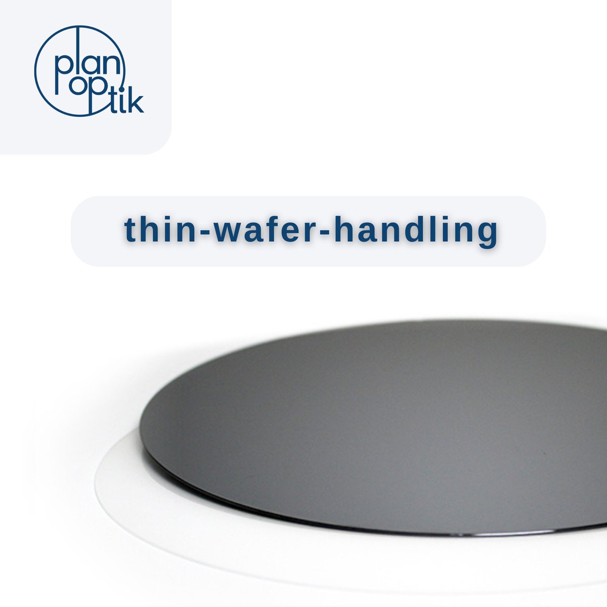
Plan Optik’s Thin-Wafer-Handling Carriers are characterized by their large number of variants and, in particular, by their stability and thus high reuse rate (typically more than 50 times).
more: https://t.co/uEP3pOSvpo
#planoptikag
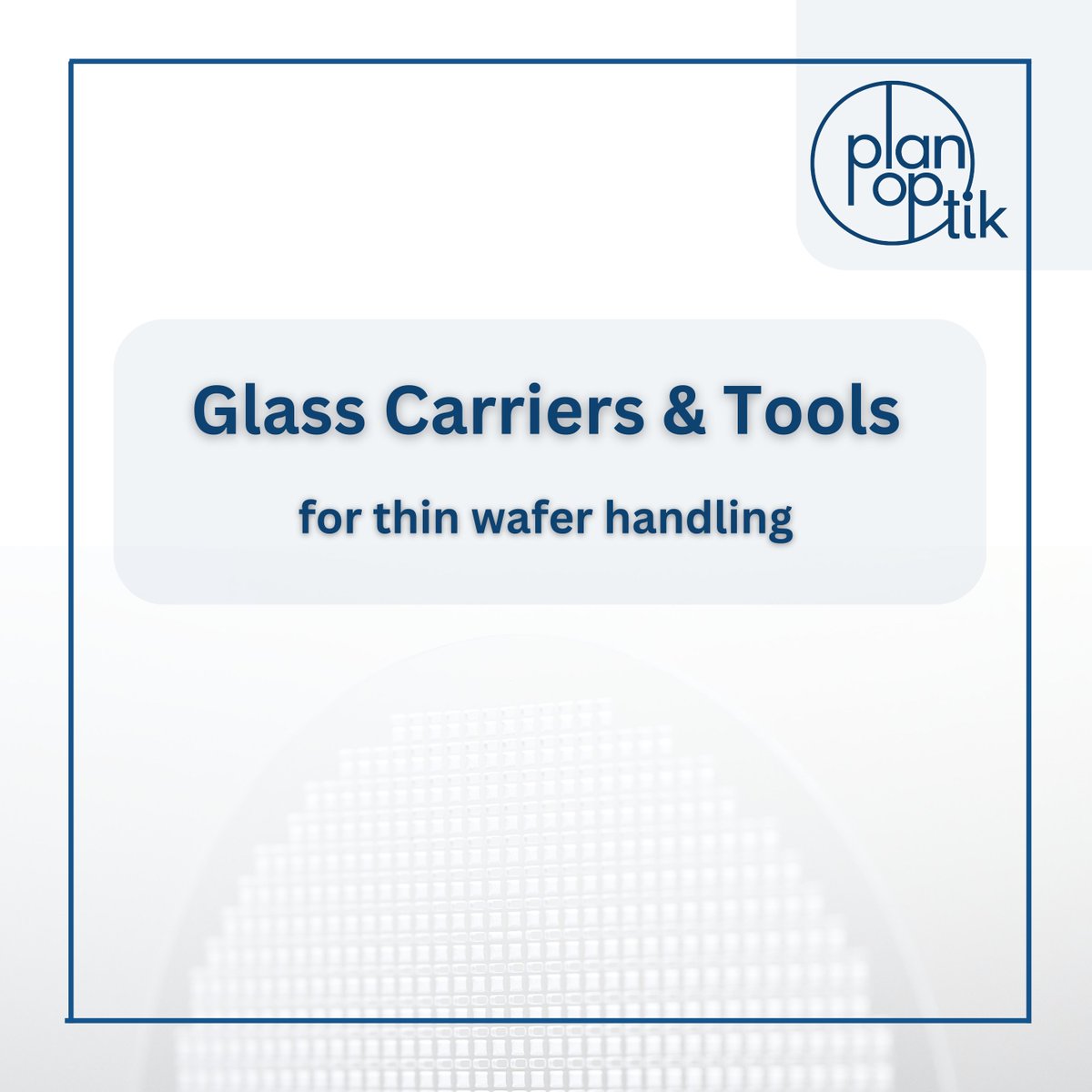
Carriers & tools for thin wafer handling from Plan Optik AG.
The wafer manufacturer produces Carrier Wafers, which can be debonded by various processes.
For more information: https://t.co/OhRayokY8S