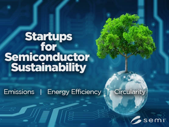
The SEMI #Startups for #Semiconductor#Sustainability program has announced 2023 semifinalists, organizations that will focus on three areas: #circularity, #emissions and #energy efficiency.
Learn more about our work to spur more green tech innovation 👉 https://t.co/jF92HheSBi
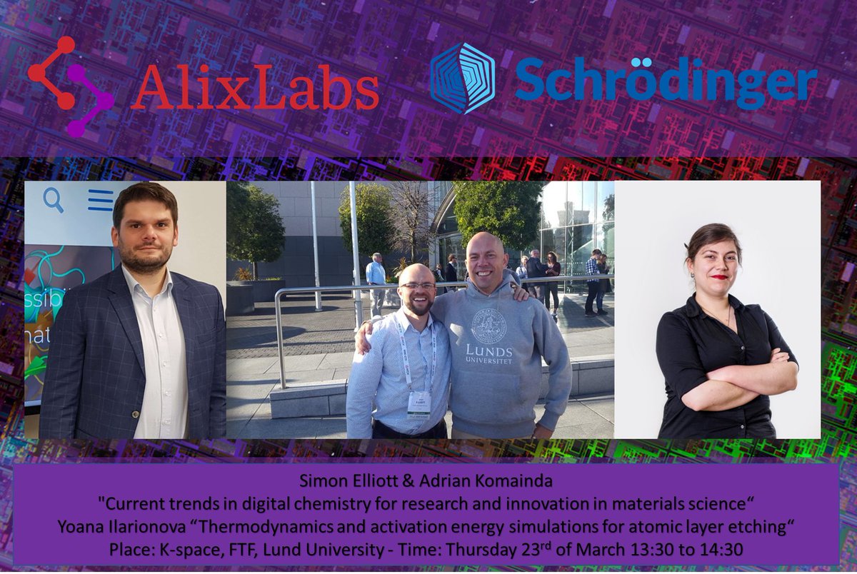
Mini-Symposium @Simon_D_Elliott & A.Komainda "Current trends in digital chemistry for research and innovation in materials science“ Y.Ilarionova “Thermodynamics and activation energy simulations for atomic layer etching“ @lunduniversity Thu. 23 March 13:30-14:30 #ALEtch#ALDep
Meanwhile, in Taipei Taiwan, our CEO Amin Karimi is busy introducing AlixLabs disruptive semiconductor manufacturing technology to the best of the best in Semiconductor manufacturing in The Taiwan Semiconductor Ecosystem.
@TaiwanInSweden#Taiwan#Sweden@DrFrederickChen
Read the story of @AlixLabs, a Swedish startup that develops a new technology to reduce the number of steps needed to create advanced #semiconductors and cut down the environmental impact of their manufacturing 🌿
https://t.co/9wUgebhXjo
Das schwedisch-sächsische Halbleiter-Unternehmen „Alixlabs“ hat weitere zehn Millionen Schwedische Kronen von Kapitalgebern erhalten. @Silicon_Saxony
https://t.co/GquL5BfOd5
AlixLabs säkrar nytt kapital till ett värde om 10 miljoner kronor - Energieffektiv klyvning av nanostrukturer på kisel lockar investerare likt Navigare Ventures och Almi Invest. #ALEtch
https://t.co/aWU0d9rwMk
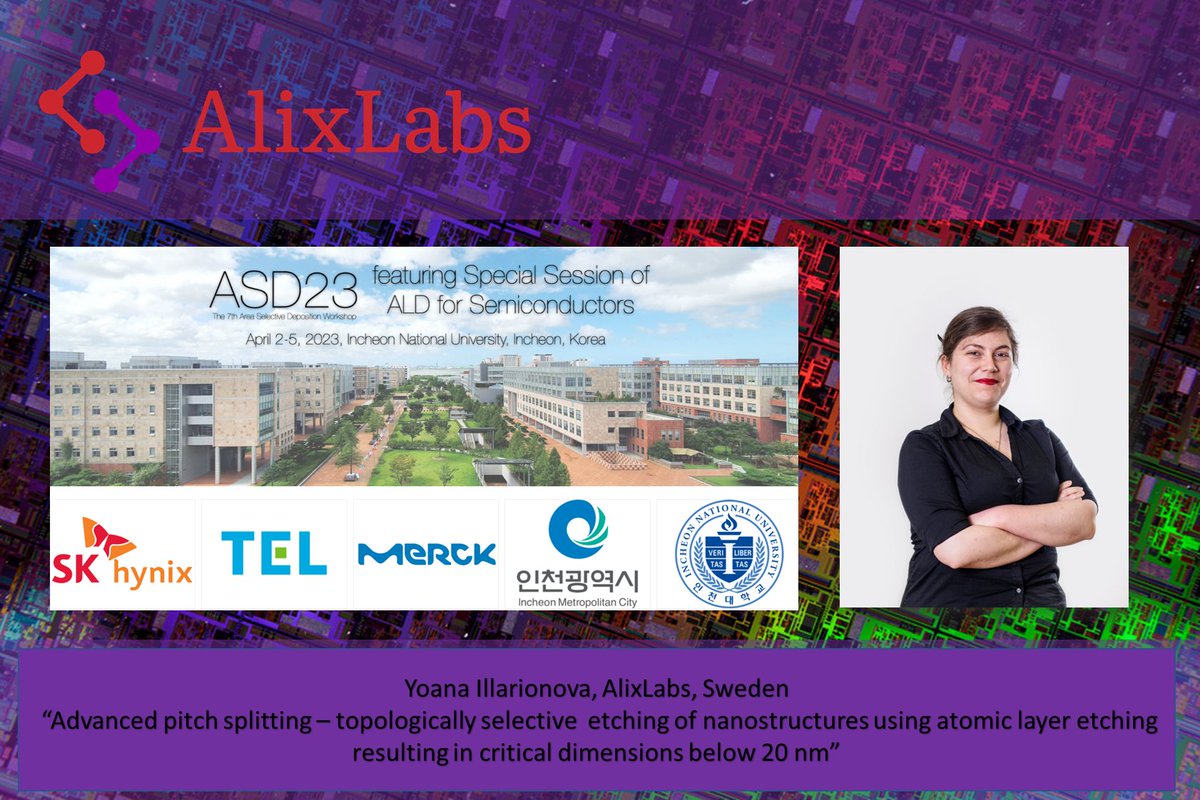
In #ALDStories, @jv3sund,CEO of AlixLabs, recalls when his team uncovered Atomic Layer Etch Pitch Splitting (APS), technology that uses a topographically selective atomic layer etching process. Learn about its potential impact on the semiconductor industry
https://t.co/XAiRGkqroV
AlixLabs announces that the company has closed a funding round of SEK 10 million. The investment comes from, among others, the Wallenberg sphere's venture capital fund Navigare Ventures, Almi Invest #ALEtch
https://t.co/FHeCXBUGZH
Using @Eulitha_AG Displacement Talbot Lithography (DTL) tool provided at @Lundsuni it is possible to produce critical feature sizes down to 60 nm with a DUV light source. We can go even further by employing AlixLabs APS technology, aiming at below 10 nm feature size #ALEtch
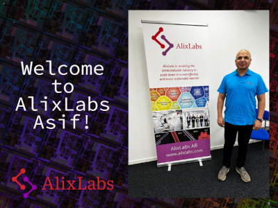
We start the new year 2023 at AlixLabs by welcoming Dr. Asif Mohammad joining AlixLabs today. Asif has a long experience in device fabrication and characterization. Welcome Asif!
AlixLabs has been rewarded with financial support from Vinnova, Sweden’s innovation agency, for further development of the company´s proprietary semiconductor patterning technology. #ALEtch https://t.co/65zQWVLPb0
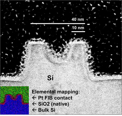
I Lund sker stordåd i små format, när AlixLabs
demonstrerar etsning av nanostrukturer på bulkkisel. Nästa steg: att bevisa att processen är gångbar även på fullstora wafers. https://t.co/GL2GoZ65KI