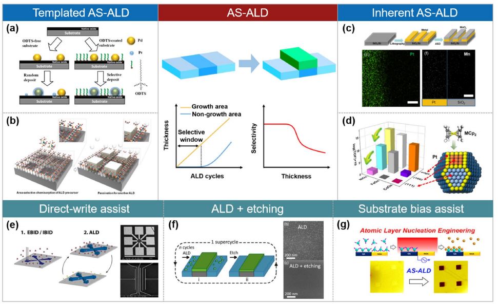
A review on atomic layer deposition (ALD) was released, which provides an introduction to ALD and highlights its applications in semiconductors, pan-semiconductors, environment and energy, and other fields. https://t.co/KD5epyKOtJ
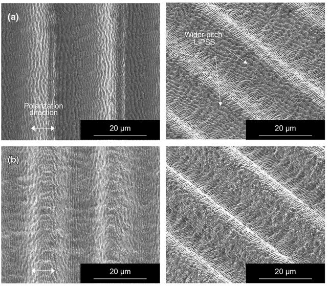
The generation of micro/nano hybrid structures on copper surfaces through femtosecond pulsed laser irradiation is achieved, which is proposed to reduce the delamination of copper lead frames from epoxy molding compounds. https://t.co/pqSXyoMB9Y
Formation mechanism of surface nanostructures of silicon carbide induced by low-energy ultrafast pulse laser was investigated. This opens a new way to reveal the subsurface dislocation defects of semiconductor wafers in a fast manner. https://t.co/cyApsCvIrN
The scanning atom lithography method and splicing atom lithography method were used to extend the structure area of self-traceable nanogratings. A perfect expansion of the grating area from 3 to 4.8 mm was achieved. https://t.co/ECiDLFARBe
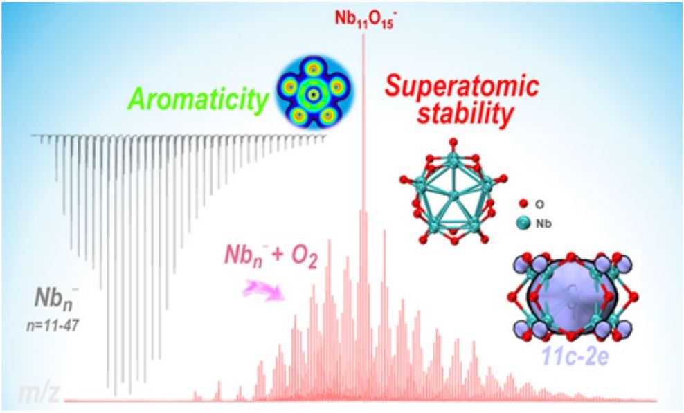
Recent progress in preparing pure metal clusters of single-atom resolution, including neutral and ionic ones, with typical examples of Al, V, Nb, Fe, Co, Ni, Rh, Pt, Ag, Cu, and Pb, was reviewed. https://t.co/hY18l8FZQw
Three paradigms of manufacturing advancement were proposed. Manufacturing Ⅲ -manipulation of material at atomic and close-to-atomic scale- is the future paradigm where atomic and close-to-atomic scale manufacturing is the leading enabling technologies. https://t.co/L3sDD5l8V2
Nanopores with diameters of 30-40 nm were fabricated on the surface of aluminum fibers through anodic oxidation under an oxalic acid system. The capillary performance of nanoporous aluminum braided wicks was tested. https://t.co/U9hyGu2wyN
A model of the distribution of grinding points corresponding to the relative motion error of the grinding wheel was developed. An error-suppression strategy was proposed by adjusting the wheel speed. https://t.co/ILokykEC5W
The DMPFIT software package for nonlinear least-squares fitting of the intensity distribution of atomic columns in atomic-resolution transmission electron microscopy (TEM) images was presented. It enables reliable and convenient atomic-scale metrology. https://t.co/6GgGCMpoKc
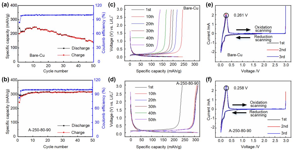
A process route of fabricating the functional surface structures on the surface of a copper collector for LIBs by twice-crisscross micro-plowing (TCMP) was proposed. Excellent surface characteristics and performance of the corresponding battery were found. https://t.co/Jp7m1JfCbk
Identification of characteristic values in impulse-based processes using small specimens were investigated. It was found that small specimens can be used for material characterization by considering the mounting parameters. https://t.co/lNlEF4EhHt
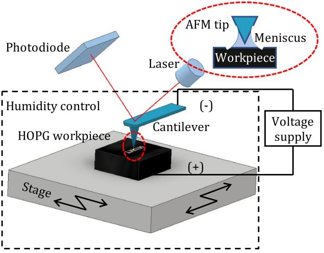
Single-atomic-layer lithography on the HOPG surface was achieved using the AFM-based electrochemical etching technique. Atomic step was obtained, indicating the promising potential of this technique for atomic and close-to-atomic scale manufacturing. https://t.co/h4tc2NBi4t
The 4th AET Symposium on ACSM and Digital Manufacturing (AETS2022) and the 8th International Conference on Nanomanufacturing (nanoMan2022) will be jointly held online on 30th August till 1st September. The details can be found via the link of https://t.co/hoHttK7rzL
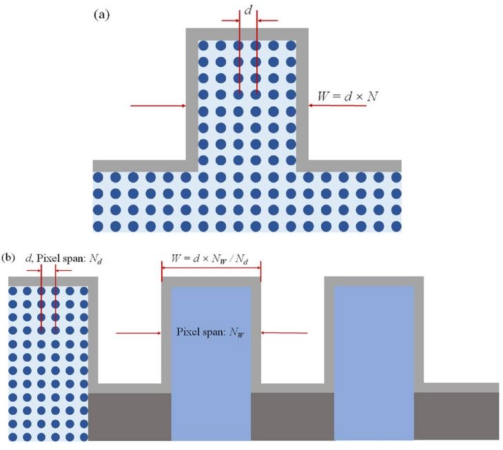
An automatic and accurate method based on a two-dimensional discrete Fourier transform was proposed for measuring the silicon lattice spacings from high-resolution transmission electron microscopy images. The efficiency of this method was confirmed. https://t.co/WP2GHf9T9Q
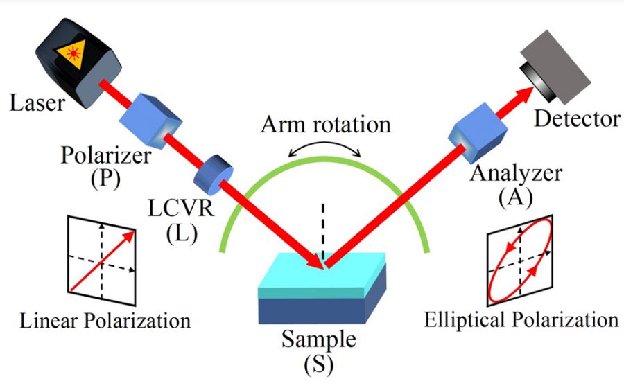
The remarkable potential of the LCVR-based polarization method for atomic film thickness measurement in ultraprecision manufacturing was demonstrated. Repeatable measurement accuracy to the sub-nanometer level was achieved. https://t.co/y5A1L4fu4J
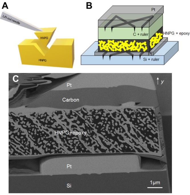
Accurate FIB-SEM 3D tomography construction of hierarchical nanoporous gold was realized by slice thickness optimization. It was found that the mean slice thickness depends on the ion beam imaging parameters. https://t.co/STr1KrCIxU
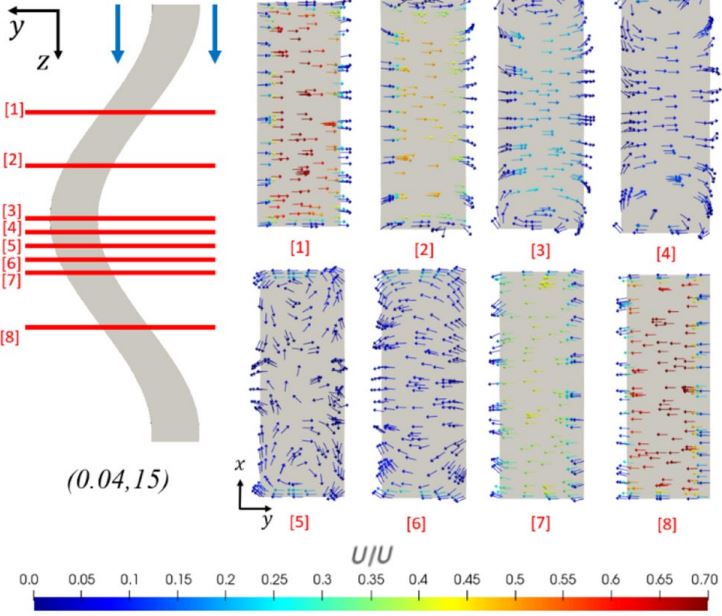
Conjugate heat transfer was numerically investigated using a three-dimensional computational fluid dynamics approach in various microchannel geometries. Cooling performance for piezoelectric ceramic stacks and spindle units was investigated. https://t.co/dHTIu9o08q
Atomic and close-to-atomic scale cutting of graphite was studied by an advanced MD simulation method. Results show that graphite can be removed with several or even single atomic layers with ultra-high machined surface integrity. https://t.co/ZfZuhX8lvX
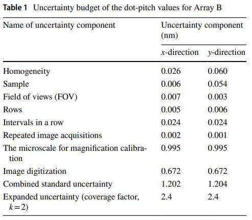
The current status of the research and development of nanodimensional standards technology, using atomic force, transmission electron, and scanning electron microscope, at the National Metrology Institute of Japan (NMIJ) was presented. https://t.co/6nxhHsrHAY
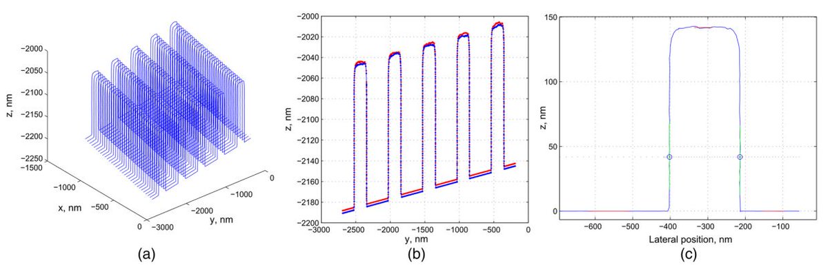
A non-destructive critical dimension atomic force microscopy (CD-AFM) approach was applied for the accurate metrology of EUV photomask. The measurement results of EUV photomask standard were verified by comparing between CD-AFM and TEM. https://t.co/t09HD3fqZa