AI is the most important inflection of our lifetime. As computing demand accelerates, the next era of innovation will depend on advances in leading-edge logic, DRAM and advanced packaging, all areas where Applied’s materials engineering expertise plays a critical role. We deliver material innovation that enables chip and packaging architectures that will power AI for years to come. #MakeItMaterial
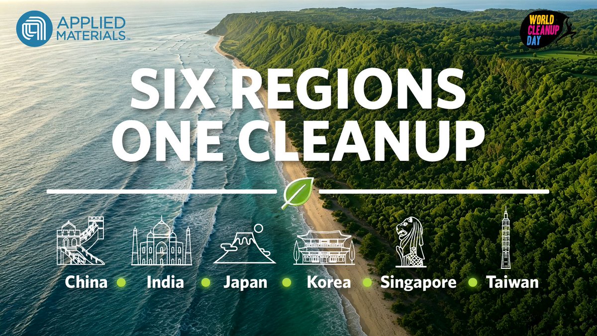
At Applied Materials, we believe that creating positive change comes not only through technological innovation, but also through long-term investment in our communities and the environment. We're conducting our Asia Cleanup Campaign for the second consecutive year, bringing together employees, community partners and nonprofit organizations across China, India, Japan, Korea, Singapore and Taiwan. Through environmental activities in rivers, wetlands, coastal areas, parks and other public spaces, we will create lasting benefits for communities and the environment.
Learn more: https://t.co/GfW4JBkZY7
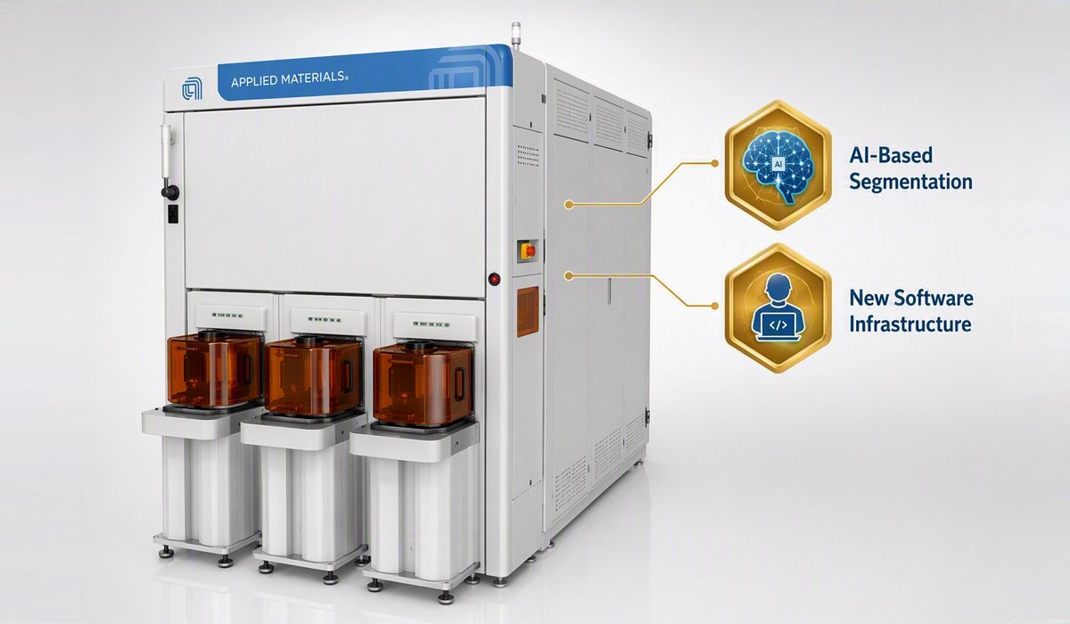
As chip packages grow in size, complexity and value, defects that were once tolerable can become costly yield killers.
Watch Dr. Lior Engel, VP of Imaging and Process Control Group, explain why the industry now needs wafer-fab-class process control in advanced packaging.
Leveraging decades of eBeam leadership, Applied Materials is helping customers improve yield and accelerate time-to-market for the next generation of AI chips. #MakeItMaterial
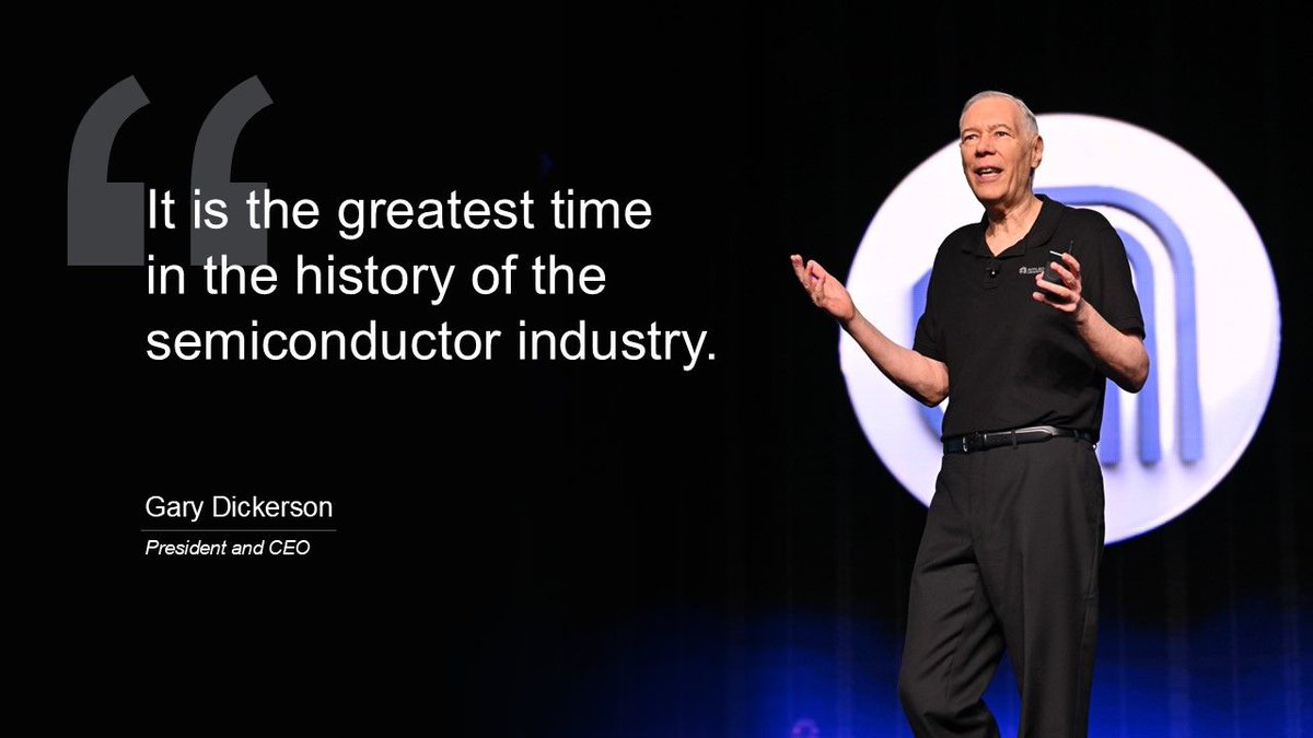
Applied Materials President and CEO Gary Dickerson recently joined CNBC’s David Faber in San Francisco to discuss how growing demand for AI computing is fueling a sustained growth cycle for the semiconductor industry, creating new opportunities for advancements in materials engineering. The discussion highlighted the critical importance of Applied in the scaling of AI infrastructure.
Watch the interview here:
https://t.co/5JLse8zTfY
We're honored to share that Applied Materials has been named one of @BusinessInsider Most Innovative Businesses in America for 2027!🏆
This ranking recognizes the top 500 U.S. corporations leading the way in R&D investment. This recognition reflects the passion, productivity and collaboration our people bring to solving the hardest problems in materials engineering. The work we do together advances the world's technology.
The semiconductor industry is at an inflection point. Logic, DRAM, and NAND devices continue to push the limits of scaling, and manufacturers are seeking new ways to improve device performance and yield while lowering cost of ownership. As High-NA EUV lithography moves from concept to high-volume manufacturing, fabs face new challenges that can affect yield, cycle time, and cost.
VeritySEM 20 is built to support these next-generation requirements, giving fabs measurement confidence on the hardest layers while sustaining precision, matching, and tool availability at fleet scale.
Learn more: https://t.co/U5PHjVZR0r
"I deeply believe material innovation will be the key to these new compute architectures for AI." - President and CEO, Gary Dickerson
At @TheSixFiveMedia summit last week, Gary framed the race for AI compute leadership as decisive for every country, industry, and company, and discussed how Applied is using AI across R&D, product introduction, operations, supply chain, and services. He emphasized that materials innovation is the key to new AI compute architectures and that the ecosystem must change how it innovates. #MakeItMaterial
The AI compute race hasn’t started. We’re still in the pregame.
@Applied4Tech CEO Gary Dickerson opened Day 3 of The Six Five Summit with @PatrickMoorhead and @danielnewmanUV on why speed to commercialization will decide who wins, and why new chipmaking approaches are key to the AI roadmap.
Watch on demand at: https://t.co/G5Z5HrDLd6
We are pleased to welcome Akash Palkhiwala to our board of directors.
As CFO and COO of Qualcomm, Akash brings extensive financial, operational and semiconductor leadership, and will also serve on the board’s Audit Committee. His strategic perspective will help strengthen Applied Materials as we continue to drive AI and advanced semiconductor technology innovation.
Read more: https://t.co/ebDOExa7ee
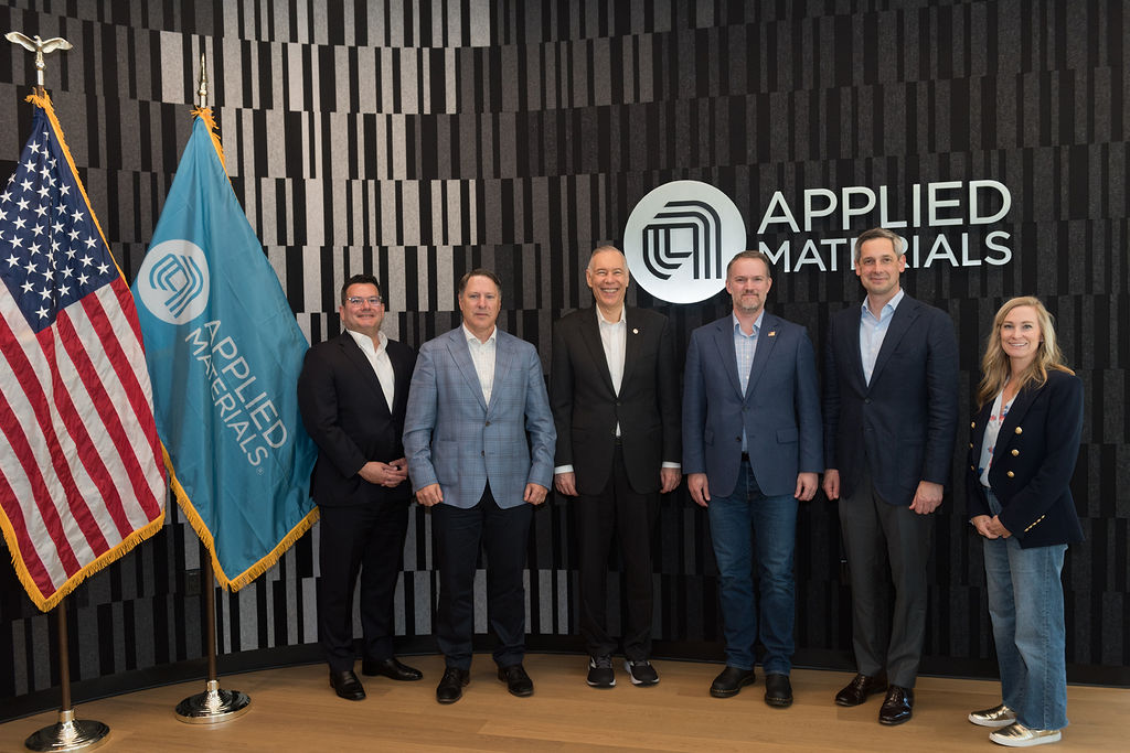
Applied Materials was honored to host @repzoelofgren to discuss our critical role in advancing semiconductor innovation and historical investment in the EPIC Center. The center is designed from the ground up to dramatically reduce the time it takes to commercialize breakthrough technologies from early-stage research to full-scale manufacturing. #MakeItMaterial
Our Q3 2026 financial results delivered another record-breaking quarter, including the highest sequential revenue growth in the company’s history. Learn more: https://t.co/boVo8hCv3C
Today we reported results for the third quarter of fiscal 2026. Check out this snapshot to learn more about our financial results and business highlights. https://t.co/boVo8hCv3C
We've announced that the University of California, Berkeley will join the company's EPIC Center in Silicon Valley as a research collaborator. Working side by side with Applied's scientists and engineers, UC Berkeley faculty and students will pursue high-impact research programs to accelerate the material and process innovations that are foundational to AI computing.
Learn more: https://t.co/TpmV7IboZy
DRAM scaling is entering a new phase shaped by Applied Materials innovations in leading-edge foundry-logic.
Watch Dr. Sony Varghese, Managing Director of Technology Strategy in the Semiconductor Products Group, explain how DRAM manufacturers are adopting technologies such as selective epitaxy, advanced copper interconnects and FinFET transistors to boost performance, power efficiency and reliability.
As AI drives demand for faster and more efficient memory, logic and DRAM technologies are creating new opportunities to accelerate the next generation of computing.
#MakeItMaterial
As AI models grow larger and more memory-intensive, DRAM density and capacity have become a critical priority for the semiconductor industry. Watch Dr. Sony Varghese, Managing Director of Technology Strategy in the Semiconductor Products Group, discuss how DRAM scaling is being enabled by EUV and how Applied’s Sym3 Y Magnum system enables more precise DRAM feature formation at scale. #MakeItMaterial
AI is the most important inflection point in our lifetime. As computing demand accelerates, the next era of innovation will depend on advances in leading-edge logic, DRAM and advanced packaging, all areas where Applied Materials and our materials engineering expertise plays a critical role. At Applied Materials, we deliver material innovation that enables chip and packaging architectures that will power AI for years to come. #MakeItMaterial
The race for energy-efficient AI isn't won at the software layer. It starts in the silicon.
DRAM and advanced packaging are two of the most critical and underappreciated levers for building energy-efficient AI systems. As data movement overtakes compute as the dominant power cost, the engineering choices we make in memory and integration define what's possible.
We're hosting a masterclass that breaks it all down: HBM stacking, hybrid bonding, 3D chiplet architectures, and the materials innovations making next-gen AI infrastructure viable.
🔗 Save your spot: https://t.co/qgdQZEAEIk
Applied Materials was proud to host U.S. Trade Representative Amb. @jamiesongreer to discuss our critical role in enabling semiconductor innovation which will advance next generation AI computing.
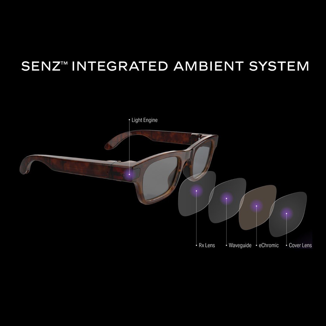
We've unveiled SENZ™ a fully integrated ambient visual platform that combines waveguide optics, light engine, sensing, vision correction, and electronic dimming in a single co-optimized system. https://t.co/aSmzmXnrft
The future of augmented reality just got a major boost and Applied Materials is announcing it where the Extended Reality (XR) industry converges.
Today at AWE, we announced a long-term joint development agreement with EssilorLuxottica to accelerate next-generation intelligent optical systems for AR and AI-powered smart eyewear.
Here's what this means:
Combining Expertise: Applied Materials' photonics and materials engineering + EssilorLuxottica's 70+ years of lens innovation = breakthrough optical platforms
The Focus: Waveguides, adaptive lens systems, and advanced materials that deliver lightweight, high-performance AR experiences
The Vision: Making smart glasses accessible, scalable, and compelling for consumers worldwide
Smart glasses won't be mainstream without a visual system that is designed from the start to optimize all the components. This partnership accelerates that timeline.
The convergence of advanced optics, AI, and wearable technology is unlocking entirely new categories of computing experiences and we're excited to lead this transformation alongside a true innovation partner.
Learn more: https://t.co/93WxO5QJ8T
#AWE2026
The surge in AI compute is accelerating the industry’s transition to advanced 3D device architectures, including gate-all-around (GAA) transistors and high-layer-count 3D NAND. To address this emerging challenge, we're introducing two new chipmaking systems designed to achieve precision processing in increasingly deep and narrow 3D structures.
Together, the new Centris™ Spectral™ SiN ALD* and Producer™ Selectra™ Mo Etch provide chipmakers with precise control over both dielectric film deposition and metal removal in high-aspect-ratio structures. The result is more uniform materials engineering at advanced nodes, enabling continued 3D scaling with better device performance, tighter process control and improved manufacturability across logic and memory applications.
Learn More: https://t.co/KRcfdtSVPB