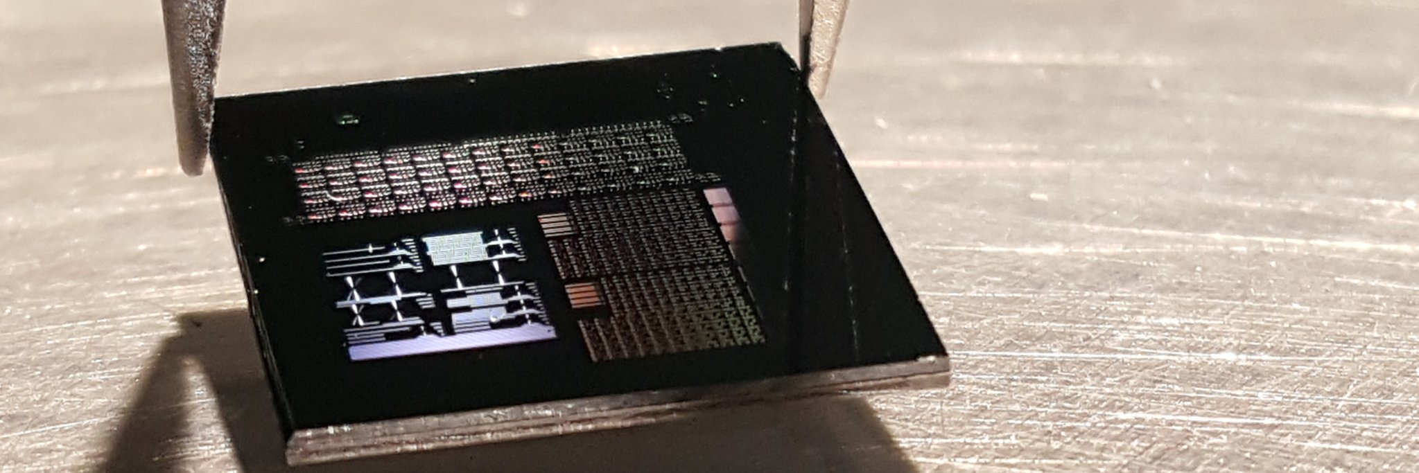
Read more here: https://t.co/re4Z05PztD Congratulations to lead authors @carloserrandoh and Mihika Prabhu & team .. And many thanks to @NSF@AFResearchLab @ArmyResearchLab @MSCActions @NDSEG@RLEatMIT
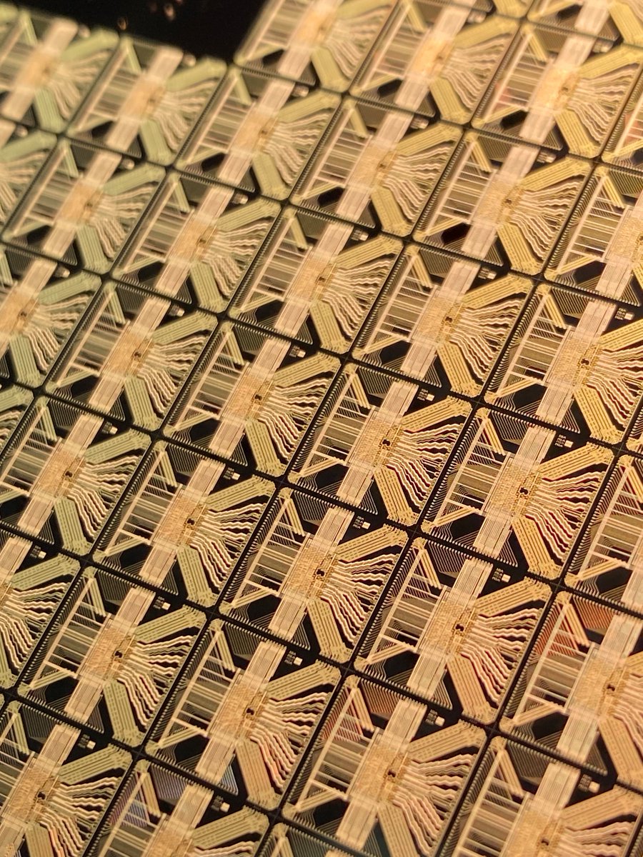
We now offer Silicon Nitride MPW runs! Our silicon nitride platform is a 400 nm thick device layer on 4.5 um buffer oxide. Small feature sizes down to 120 nm, rapid turnaround with passive devices shipped within 4 weeks. https://t.co/ot2j12zYtS
#optics#nanotechnology
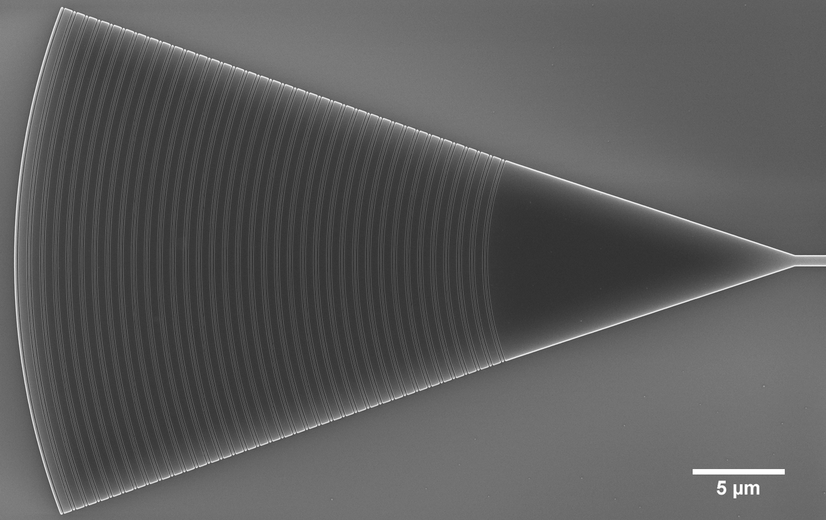
Unlike glass lenses, metallic lenses such as this gold multi-layered Fresnel zone plate use diffraction and not refraction to focus light. They are only the width of a human hair and are often used to focus extreme ultraviolet and X-ray wavelengths.
#xray#Optics#nanotechnology
Did you know that we also fabricate interposers? Interposers are used to connect photonic integrated circuits to PCBs. Our interposers are custom-made for your requirements. Details are available on our website at https://t.co/XtEGr3KGO1
#photonics#electronics#Engineering
Version 5 of the NanoSOI Process Design Kit is here! Update your PDK for our October 5th multi-project wafer run.
This release includes new features, such as new grating couplers and support for waveguide routing. What other components or tools would you like to see? #photonics
The main challenge of extreme ultraviolet optics is most materials are opaque to short wavelengths. To overcome this, we offer free-standing optics, including zone plates, gratings, and calibration standards. What applications would you use these in? #Optics#Engineering#Science
We look forward to participating in the upcoming conference ICXRL20 (https://t.co/M0T9pU7mFI) on December 8-10. This conference relates to advanced extreme UV and X-ray sources, and their application in physics, (bio-)chemistry, and materials science. #icxrl20
The editorial of our May 2020 issue discusses how integrated quantum photonic chips offer the promise of a convenient, scalable platform for performing tasks, such as quantum communication and information processing.
https://t.co/b6fEeHJLqo
🧬🗞️
Three NSERC-backed researchers from @UWaterloo are developing a DNA-based #vaccine that can be delivered through a nasal spray and will work by using bacteriophage, allowing the vaccine to replicate within bacteria already in our body.
Details ▶️ https://t.co/Tr18gAIgmm
The #OFC20 exhibition is now open! Come visit booth 4019 to watch our live PIC demo and learn about our photonics multi-project wafer runs and custom fabrication capabilities! #siliconphotonics#OFC2020
The #OFC20 exhibition is now open! Come visit booth 4019 to watch our live PIC demo and learn about our photonics multi-project wafer runs and custom fabrication capabilities! #siliconphotonics#OFC2020
It is not too late to sign up for our public webinar covering our lesser-known photonic circuit fabrication capabilities at Applied Nanotools! Webinar Topic: Custom PIC Processing Options. Friday at 6 pm GMT. Registration link is here: https://t.co/HTVkYU6VQ4
NANOvember kicks off in Edmonton with Lab2fab 2019! Opening remarks were followed by a presentation from Simon Doe, National Facility Manager, @AnffSa.
Attend our public webinar on November 8th! We will be presenting our capabilities for photonic integrated circuit fabrication, and providing an overview of the submission process. Visit here to register: https://t.co/Uzl8pOBUVp
We are pleased to announce @AppliedNT will be exhibiting at NANOvember in Edmonton, Alberta. Thanks for your support! Learn more about the three complementary events CMC is hosting with @Nano_Canada from Nov 4 - 6, 2019: https://t.co/kmNTH3Z9um
Although not likely to be ready for commercial production, here is a short slideshow of some of R&D we are involved with at Applied Nanotools in our X-Ray Optics division for zone plate optics. #xrays#zoneplates
https://t.co/U2yGBdq2aY
We're back again at the #Spie Optics + Photonics conference this year. Come learn about some of our recent advances in X-ray Optics and Integrated Photonics. https://t.co/USqaf9KKxa