Today, EV Group launched the redesigned EVG®150 automated resist processing system, which provides greatly improved throughout and many additional features in a smaller-form-factor, universal platform.
Find out more here: https://t.co/YH4icWU4uA
We're proud to announce a collaboration with Toppan Photomasks, Inc. with the goal to foster industrial-scale implementation of Nanoimprint Lithography for high-volume manufacturing in the photonics industry. Read on to find out more! https://t.co/E8hh6JWvhh
Today, we're proud to announce our revolutionary NanoCleave™ IR Layer Release Technology, which enables nanometer-precision layer transfer through silicon, eliminating glass substrates for advanced packaging and enabling thin-layer 3D stacking.
https://t.co/2oA9zVmVWo
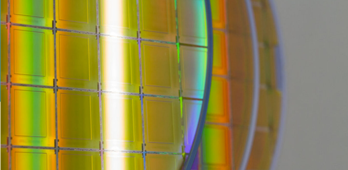
ITRI joined hands with @EVGroup (EVG), an Austrian leading supplier in the semiconductor industry, to develop advanced heterogeneous integration processes. The ITRI-EVG collaboration can help improve the performance and functionality of chips. Read more: https://t.co/ErzQaA3rV9
The new issue of @Semi_Dig is out - have you read our article by Thomas Uhrmann on "Emerging Metrology Requirements for Heterogeneous Integration and 3D Packaging?" https://t.co/IMxh7qoMfU
It's all systems go this week at ANFF-SA with deliveries of new equipment including our new @EVGroup spin coater! Safely delivered by Fleurieu Cranes for our nearly completed cleanroom facility! Exciting times! @ @FlindersCSE @sachiefsci
@KhairyKhalil1 A good question indeed - and best to ask your car's manufacturer directly. We are a semiconductor equipment manufacturer and don't have much expertise in the field of charging EVs - other than providing charging stations for our employees ;)
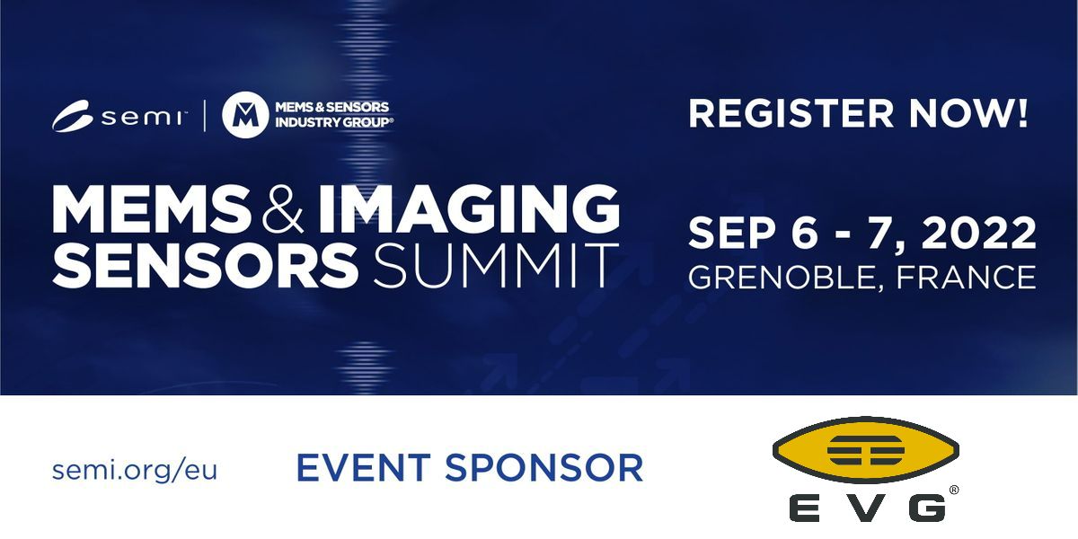
We are delighted to have @EVGroup as a sponsor of the MEMS & Imaging Sensors Summit on Sep 6-7, 2022! Join us in #Grenoble, France, and learn more about Intelligent Sensing for Better and Smarter Living. https://t.co/tbYD8pQ26z
#MEMS#imaging#sensors#WeThankOurSponsors
Interested in MEMS/nanotechnologies? Join @EVGroup's FREE technology webinar to learn about their cutting edge solutions for the auto, industrial, consumer & emerging markets.
Thur Mar 24 at 6pm (AEDST)
Register: https://t.co/Z0jKYlzt8r
@UniSAFII @FlindersCSE @UniofAdelaide
Breakthrough in wafer-level optics technologies made possible by EVG’s NILPhotonics® Competence Center: The collaboration with Teramount helps solve a key challenge of connecting many fibers to silicon chips for datacom and telecom applications! https://t.co/ug8fLf8WTf
We're proud to announce having received the "Supplier Excellence Award" from the Korea National NanoFab Center (NNFC), during a ceremony held on January 26.
Read more: https://t.co/PNRRRIA0Hm
We're honored to be recognized by @boschglobal as a Preferred Supplier in the field of #semiconductor for our leading process equipment and comprehensive customer support https://t.co/6wIURvzB1R #MEMS#sensors
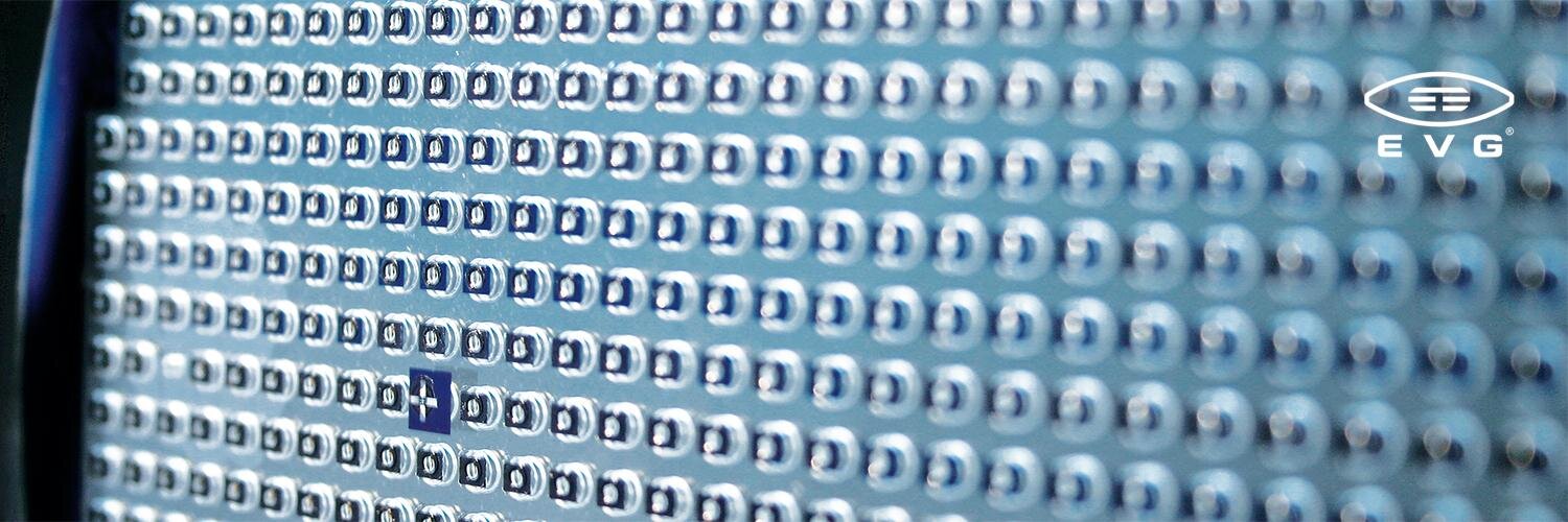
Nanoimprint lithography (NIL), lens molding and lens stacking (UV bonding), in a single platform?
Look no further than the EVG®7300, EVG's most advanced system to combine multiple UV-based processes.
https://t.co/1HGXMW7LmN
"Lithography and bonding equipment drives More-than-Moore technology innovation" – Yole Développement and EVG's Thomas Uhrmann sat down for an interview:
https://t.co/g10gORZgO5