MOSFET Logic Gates – Part 1: NOT & AND ⚡
We’re kicking off a series on MOSFET‑based logic gates, covering the five fundamentals:
🔹 NOT
🔹 AND
🔹 NAND
🔹 OR
🔹 NOR
Part 1 focuses on the building blocks – the NOT (Inverter) and AND gates.
We’ll look at MOSFET operation, visualize current flow with LEDs, and summarize key logic behavior.
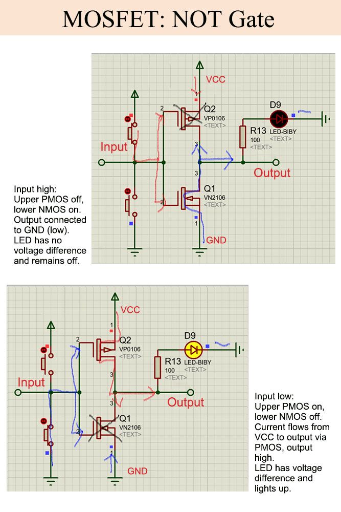
1️⃣ NOT Gate (Inverter)
📌 1 input → 1 output
Logic:
▪ Input HIGH → Output LOW
▪ Input LOW → Output HIGH
MOSFET operation:
▪ Input HIGH → Upper PMOS off, lower NMOS on → Output pulled to GND → LED off
▪ Input LOW → Upper PMOS on, lower NMOS off → Output pulled HIGH → LED lights
💡 Tip: Trace the current – only the active MOSFET conducts, creating the correct voltage across the load.
Key takeaways:
Simple inverter – output flips the input
PMOS pulls HIGH, NMOS pulls LOW
2️⃣ AND Gate
📌 2+ inputs → 1 output
Logic:
▪ Output HIGH only if all inputs HIGH
▪ Any input LOW → Output LOW
MOSFET operation:
▪ All HIGH → NMOS network conducts → Output HIGH → LED lights
▪ Any input LOW → NMOS network incomplete → Output LOW → LED off
💡 Tip: Think of the NMOS network as a chain – breaking any link breaks the output.
Key takeaways:
Requires all inputs HIGH to activate
MOSFET principle: PMOS pull‑up, NMOS pull‑down
📌 DFM Tips for PCB Layout
Keep NMOS pull‑down paths short and wide
Use series resistors with LEDs to prevent overcurrent
Avoid unnecessary crosstalk between inputs
❓ Which of these two gates do you find easier to implement on a PCB?
Drop your thoughts in the comments 👇
#MOSFET #LogicGate #NOT #AND #CMOS #PCBDesign #SMT
#PCBSync #PCBDesign #Electronics
🚀 In modern automation, communication isn't just about sending data — it's about sending it accurately, consistently, and over long distances.
#PCBSync#PCBassembly#pcbmanufacturer#pcbdesign#pcb#pcba#circuitboard#electronics
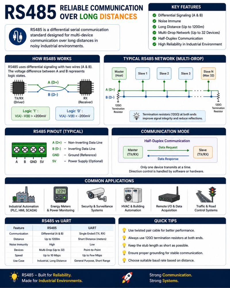
That’s why RS485 remains a go-to standard in industrial communication. 🔌
Unlike basic serial protocols, RS485 uses differential signaling (A(+) and B(-) lines), transmitting data based on the voltage difference between the two lines. This design delivers outstanding immunity to electrical noise and signal interference.
✅ Key benefits:
Communication distance up to 1200 meters
Supports multiple devices on the same bus
High resistance to electromagnetic noise
Reliable operation in harsh industrial environments
Ideal for half‑duplex and multi‑drop networks
🔧 Common applications:
PLC & SCADA systems
Energy meters
HVAC controllers
Industrial automation panels
Remote monitoring systems
Building management systems
💡 Speed is impressive.
💡 Reliability is powerful.
In environments where failure is not an option, communication must be strong, stable, and dependable — and RS485 continues to deliver exactly that.
#EmbeddedSystems #RS485 #IndustrialAutomation #PLC #SCADA #Automation #Electronics #CommunicationProtocol #Engineering
One BJT, Three Amplifiers: Which Terminal Is Common?
Your sensor output looks fine on the scope. Connect the next stage and the voltage drops. Before adding gain, check whether the load is pulling the signal down.
The three BJT amplifier configurations solve different problems:
Common emitter (CE): Base in, collector out. Use it for voltage gain when an inverted output is acceptable.
Common base (CB): Emitter in, collector out. The output voltage stays in phase. Check that your source can drive the low input impedance.
Common collector (CC): Base in, emitter out. The emitter follower has voltage gain close to 1 and is useful as a buffer when the next stage would otherwise load the source.
The shortcut: “Common” tells you which terminal the input and output share as their AC reference.
If your sensor voltage sags when you connect the next stage, what would you measure first to confirm a loading problem?
#PCBSYNC #BJT #AnalogDesign #AmplifierDesign #ElectronicsEngineering #CircuitDesign
MOSFET ringing – when the clean PWM signal you designed isn’t what you get on the board.
In theory, your PWM waveform looks perfect.
In reality – once it reaches the MOSFET gate – small oscillations often appear after the rising or falling edge. That’s ringing.
🔴 It’s not just a waveform glitch
It’s easy to ignore ringing as a minor scope artifact. But if the peaks get too high, you can face:
Gate overstress
Unpredictable switching
Higher losses and heating
Worse EMI performance
This isn’t about aesthetics – it’s about reliability.
🔴 Common root cause: parasitic L & C
Ringing usually comes from the combination of:
MOSFET capacitance
Parasitic inductance in the gate-drive loop
Fast voltage/current transitions
Even a clean PWM source can produce ringing at the board level.
🔴 The PCB is often the culprit
A gate-drive loop that’s physically too large = more parasitic inductance.
Long traces, loose return paths, excessive driver–MOSFET spacing → ringing.
This is a layout problem, not just a MOSFET problem.
🔴 Start with physical fixes
Before adding exotic solutions, try:
Place the driver as close as possible to the MOSFET
Minimize gate loop area
Shorten traces and optimize return paths
Add or adjust a gate resistor to dampen oscillations
A small gate resistor often helps – but don’t overdo it. Too much resistance slows switching and increases loss.
🔴 Protection ≠ root-cause fix
Yes, a TVS or clamp can limit voltage spikes. But that’s protection, not a solution to poor layout or drive-loop design. Fix the cause, not just the symptom.
💡 Key takeaway
A perfect PWM signal at the controller doesn’t guarantee a clean waveform at the MOSFET.
What looks like a square wave on the schematic can behave very differently on the board.
Treat ringing as both an electrical and a physical design problem.
#PCB #MOSFET #PowerDesign #HardwareEngineering #ElectronicsEngineering #CircuitDesign #PCBDesign #EMC
#PCBSync #PCBDesign #Electronics
USB Communication Basics: PCB Layout & Routing Notes That Actually Matter 💡
#PCBSync #PCBassembly #pcbmanufacturer #pcbdesign #pcb #pcba #circuitboard #electronics
USB is everywhere in embedded design.
But in practice, most USB issues aren't protocol problems — they're layout and routing problems.
Here's a quick refresher on USB basics + the PCB rules that separate working prototypes from field failures.
🔹 USB communication in simple terms
USB handles both data and power over the same cable.
Host (PC, hub) initiates all communication
Device (MCU, peripheral) responds
Data travels over a differential pair (D+/D−)
Common versions to know:
→ USB 2.0: 480 Mbps, still the workhorse
→ USB 3.x: higher speed, extra pairs
→ USB Type‑C: reversible, now mainstream
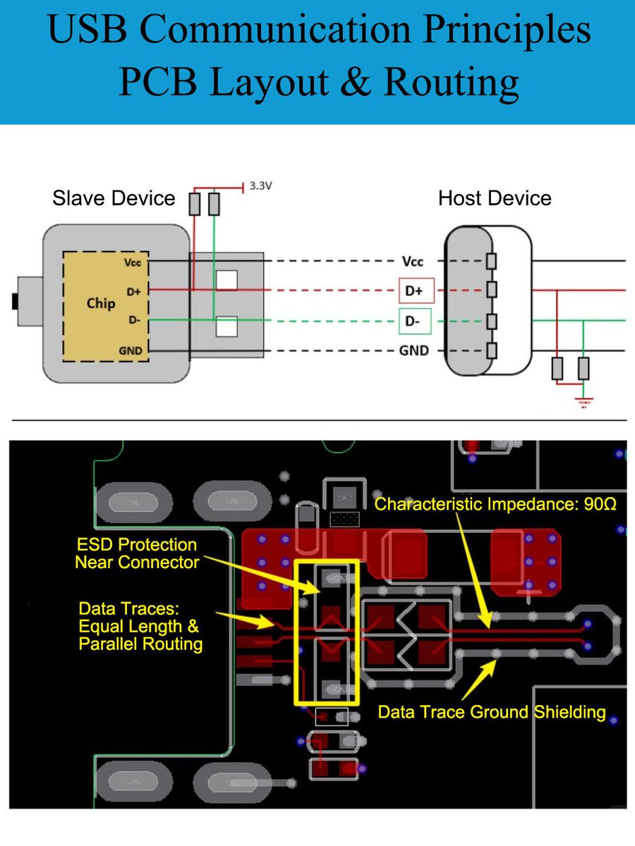
🔹 Key PCB layout guidelines
1️⃣ Component placement first
USB connector close to board edge
MCU close to connector → short data traces
ESD protection as close to connector as possible (limits ESD current from entering the PCB)
2️⃣ Routing rules for D+/D−
Route as a matched differential pair
Keep equal length, parallel, constant spacing
Target 90Ω differential impedance
Avoid sharp corners, stubs, and unnecessary detours
3️⃣ Ground reference & shielding
Solid ground plane under the USB pair
Add ground shielding if routed on outer layers
Never split the ground under USB signals — a clean return path is critical
4️⃣ Via usage
Minimize vias on D+/D− (each via adds impedance discontinuity)
If vias are unavoidable, keep them symmetric on both lines
🔹 Common mistakes that kill USB
❌ Routing USB next to switching power traces
❌ Long, winding D+/D− routes
❌ ESD protection placed far from connector
❌ Broken or noisy ground under the USB pair
Result: enumeration failures, unstable connections, or EMC headaches.
🔹 A DFM reality check
Poor impedance control → board‑to‑board variation
Excessive vias → lower yield at higher speeds
Clear stack‑up definition is required for consistent 90Ω differential impedance
"Good design is buildable design."
What's the strangest USB layout issue you've debugged? 👇
#PCBDesign #USB #HighSpeedDesign #SignalIntegrity #HardwareDesign #DFM
Not every antenna design works perfectly on the first try.
Today, while analyzing S11 (Return Loss), I noticed something fascinating.
At first glance, it’s just a curve.
But if you look deeper, it tells a complete story:
📊 The dip reveals the resonance point.
📡 Values below -10 dB indicate good impedance matching.
📶 The highlighted region defines the operational bandwidth.
Here’s the real insight:
Even a small tweak in design parameters can shift the entire curve—and completely change performance.
That’s the beauty of RF engineering.
It’s not just about getting results. It’s about understanding why they behave the way they do.
#PCBSync #PCBDesign #Electronics
MOSFET Gate Resistor: Why It Matters & How to Choose It ⚡
#PCBSync #PCBassembly #pcbmanufacturer #pcbdesign #pcb #pcba #circuitboard #electronics
When designing power electronics, it’s easy to focus solely on the MOSFET. But a tiny component between the driver and gate—the gate resistor (Rg)—deserves just as much attention.
Why? Because Rg directly impacts switching behavior, efficiency, and EMI.
🔹 What does the gate resistor do?
Placed between the driver output and MOSFET gate, Rg:
• Limits peak gate current
• Controls switching speed (dv/dt, di/dt)
• Reduces EMI and ringing
• Protects the driver IC
• Helps prevent parasitic turn-on
🔹 Gate current & driver power
Peak gate current ≈ Vdrive / (Rdriver + Rg)
Driver power ≈ ½ · Qg · Vdrive · fsw
Always ensure peak current stays within driver limits. And don’t overlook the gate charge curve and Miller plateau when selecting Rg.
🔹 Efficiency vs. EMI – the classic trade-off
• Large Rg → slower switching, higher loss, lower EMI
• Small Rg → faster switching, lower loss, higher EMI
The right value is almost always a conscious balance, not an extreme.
🔹 Practical tips
✅ Use separate turn-on (RGon) and turn-off (RGoff) resistors – a diode can create two paths. A good starting point: RGon ≈ 2 × RGoff
✅ Watch for gate loop inductance – fast di/dt can cause voltage spikes. Rg helps dampen oscillations.
✅ Beware of the Miller effect – drain voltage transitions can couple through Cgc and cause parasitic turn-on, especially in half-bridges.
🔹 Layout matters
• Place Rg as close as possible to the MOSFET gate
• Minimize gate loop area
• Keep gate traces short
• Use Kelvin source connections where feasible
Takeaway – The gate resistor is small in size but huge in influence. Choose it wisely, and pair it with good PCB layout for stable, efficient switching.
#PowerElectronics #MOSFET #HardwareDesign #EMI #PCBDesign #EngineeringTips
How a simple diode demodulates AM signals 📻
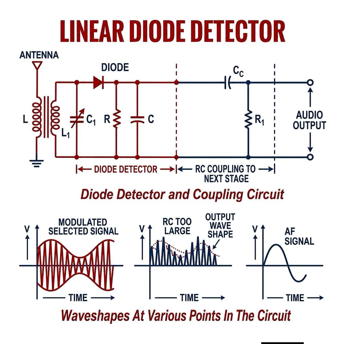
Ever wonder how your radio extracts audio from a modulated carrier wave? Here’s a quick breakdown of the classic linear diode detector:
The antenna and tuned LC circuit select the desired radio frequency.
The diode rectifies the signal, passing only one half of the waveform.
This creates a pulsating DC that still follows the original envelope of the AM signal.
An RC network smooths the waveform by filtering out the high-frequency carrier, leaving the slower-changing audio.
A coupling capacitor and resistor then pass only the audio component, removing DC and preparing it for amplification.
⚠️ Design tip: If the RC time constant is too large, distortion creeps in—the circuit can’t keep up with rapid envelope changes.
Simple, elegant, and still relevant in many RF designs.
#RFDesign #Electronics #AMRadio #EngineeringBasics
#PCBSync #PCBDesign #Electronics
Choosing the right microcontroller can make or break your robotics, IoT, or AI project. 🎯
#PCBSync#PCBassembly#pcbmanufacturer#pcbdesign#pcb#pcba#circuitboard#electronics
Performance, cost, and learning outcomes all hinge on this one decision. Yet many students and educators struggle to know where to start.
I’ve created a simple visual guide that breaks down the most widely used microcontrollers and their ideal use cases:
🔹 Arduino Uno – Best for beginners & foundational learning
🔹 ESP32 – Go-to for IoT, AI, and wireless communication
🔹 ESP8266 – Low-cost solution for basic Wi-Fi projects
🔹 Arduino Nano – Compact, great for small robotic systems
🔹 Raspberry Pi Pico – Fast, affordable, excellent for embedded learning
🔹 STM32 – Industrial and high-performance applications
🔹 ATtiny85 – Ultra low‑power, compact designs
🔹 Teensy – High‑speed, real‑time processing
Quick recommendations:
👉 Beginners → Arduino Uno or Nano
👉 IoT projects → ESP32
👉 Advanced robotics → STM32
👉 AI / voice systems → ESP32 or Raspberry Pi Pico
As a Robotics and STEM educator, I’ve seen how clear, early guidance builds students’ confidence and sparks innovation. That’s exactly why I put this poster together — to make complex concepts more accessible and help learners pick the right tool for the job.
What’s your go-to microcontroller for teaching or building? Let me know in the comments. 👇
#Robotics #IoT #ArtificialIntelligence #STEMeducation #Microcontrollers
GaN isn’t always the better choice.
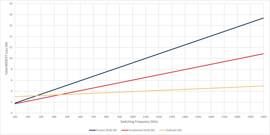
We hear a lot about how GaN FETs are replacing silicon across the board. But below ~500 kHz, an optimized silicon MOSFET pair can match—or even beat—GaN on total losses, while being significantly easier to design with.
Here’s why:
🔹 GaN’s real advantage is switching loss (near-zero Qrr, low Qgd, negligible Eoss). At 1 MHz, that’s a huge win. At 200 kHz, you’re paying that penalty five times less often, and the gap shrinks accordingly.
🔹 Conduction loss doesn’t care about frequency—it’s all about RDS(on) and duty cycle. In a given package, the best silicon MOSFETs often match or beat GaN on RDS(on), thanks to decades of process maturity.
Take a real-world example:
12V → 1.8V, 20A converter at 500 kHz.
Optimized silicon pair (low-Qgd high side + low-RDS(on) low side): 3.63W
EPC2045 GaN pair: 3.42W
That’s a 0.21W saving with GaN (~0.6% efficiency), in exchange for:
A dedicated GaN gate driver with tight voltage tolerance
No avalanche rating (tighter layout requirements)
All heat exiting through solder bumps into the PCB
Below 450 kHz, the silicon pair actually wins—switching losses keep dropping while conduction losses stay constant. Above 1 MHz, GaN pulls away decisively.
Bottom line:
GaN makes sense for high frequency, tight thermal constraints, or minimal footprint. But if you’re switching at 200–400 kHz with reasonable board space, optimized silicon is simpler, cheaper, and just as efficient.
Not every narrative holds up under the math. What’s your experience—have you found a crossover point where GaN became the clear winner in your designs?
#PCBSync #PCBDesign #Electronics