Bengaluru is arguably one of the luckiest places to live for a heritage lover like me
We often get absorbed in the noise of the “Silicon Valley” narrative, but beneath the glass facades, flyovers, and traffic, history waits patiently.
Within the city—and just a day’s drive beyond it—you don’t need a time machine to touch the past.
You only need to look.
The true magic of Bengaluru is not limited to its famous monuments. It lies hidden in plain sight, seamlessly woven into everyday life:
• Inscriptions older than modern languages, etched into walls we pass without notice.
• Veeragallu (hero stones) standing quietly at street corners, remembering sacrifices made a thousand years ago.
• Forgotten shrines and stepwells tucked behind modern buildings, holding both water and memory.
• Sacred hills that witnessed dynasties rise and fall long before the first tech park existed.
But the real privilege? The treasure chest that opens up if you drive just 2-3 hours in any direction.
Here are just a few heritage gems you can cover in a single day:
📍 Bhoga Nandeeshwara (Nandi Village):
Forget the sunrise view on the hill; the real marvel is at the base. A complex that serves as a textbook of Karnataka’s history—starting with the Nolambas, expanded by the Cholas and Hoysalas, and fortified by the Vijayanagara emperors. A millennium of art in one compound.
📍 Agrahara Bachahalli & Sindhaghatta
📍 Nuggehalli, Kambadahalli & Mosale , Basaralu , Nagamangala
📍 Avani & Kolar:
Avani offers the stunning Nolamba style of architecture. Nearby, the Virupaksha , Kolaramma and Someshwara temples showcase the heavy, majestic influence of the Cholas and Vijayanagara styles right in our backyard.
📍 Kaidala (Tumakuru):
Home to the Channakeshava temple and a rare masterpiece by the master sculptor , hidden away in a quiet village.
📍 Begur (Within the City):
You don’t even need to leave the ORR to see the roots of the city. The Panchalingeshwara temple here houses the 9th-century inscription that has the word "Bengaluru” and ancient Ganga era Architecture
📍 Aralaguppe , Turuvekere , Nagalapura, Vignasanthe, Kunigal, Tandaga and Nonavinakere
You don’t need flights, long weekends, or elaborate itineraries.
Just curiosity, a little time, and the willingness to pause.
For those who truly listen, Bengaluru doesn’t just grow—it remembers.
#Bengaluru #NammaBengaluru #KarnatakaHeritage #IndianHistory #Hoysala #Chola #Vijayanagara #HiddenHeritage #Veeragallu #Inscriptions #SacredLandscapes #IncredibleIndia @KarnatakaWorld@ChristinMP_
To drive strategy execution, leaders should instead set goals that are FAST — frequently discussed, ambitious, specific, and transparent.
Learn more: https://t.co/BGL2cIShn1
If you have ever taken that “road” you know it is not a road, never tarred. Lorry’s use it for transporting mud, now folks use it to cut short their travel time and then can’t blame that it is a pothole riddled “road”. Bangalore infra needs attention but let’s not get carrier away.
Boost SVA productivity with Questa One SFV PropertyAssist. #AI + #Formal = faster, safer assertions. Watch the webinar and demo: https://t.co/bLZTcPz2WY
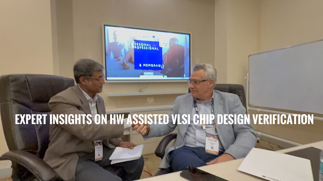
Hyperscalers and Custom Silicon: Siemens’ Jean-Marie Brunet on the Future of Semiconductors
At DVCon India 2024, Jean-Marie Brunet, VP & GM of Hardware-Assisted Verification at Siemens Digital Industries Software, shared transformative insights with EEHerald on the global semiconductor landscape. Highlighting the surge in wafer capacity, the rise of hyperscalers building purpose-built chips, and advancements in verification for 2nm nodes and beyond, Brunet underscored Siemens’ role in tackling design complexities.
Key Trend: Geopolitical shifts are driving investments in advanced nodes, with players like Intel, TSMC, Samsung, and Japan’s Rapidus expanding capacity. “It’s exciting to see Japan investing in fabs and advanced nodes,” Brunet said, noting TSMC’s continued leadership.
https://t.co/SZ2iNDKmXv
#DVCONIndia #Semiconductors #CustomSilicon #EDA #Siemens #Innovation
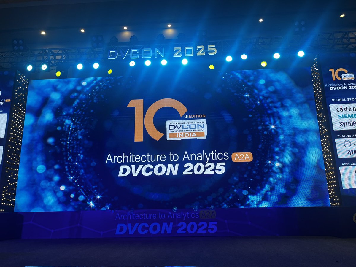
DVCON India 2025 marks its 10th year as the premier hub for India’s semiconductor & VLSI design community! With 20% of global chip designers in India. Organized by Accellera, connects innovators, EDA tools, and silicon-proven IPs. This year’s event set new benchmarks with young talent, expanded exhibits, and cutting-edge themes like “Chiplets, GenAI, and Beyond” showcased at TCS’s booth. #DVCONIndia2025 #Semiconductor #VLSIDesign #Innovation
https://t.co/uGy8LkVN4m
⏳ Early Registration Ends September 12, 2025!
Don’t miss DVCon Europe 2025—Europe’s leading conference for chip architects, #design & #verification engineers, and IP integrators.
🔗 Register now: https://t.co/HgPkvaCXwM
UCIe 3.0 is here. Discover how Siemens EDA helps teams verify smarter with Questa One Avery VIP. Read the white paper for details: https://t.co/tQwFcQx9Si
Unified simulation is here. Questa One Simulator combines functional, fault & DFT engines into one smart, AI-powered solution. https://t.co/fecRrwRUXC
🎓 Siemens, @Arm & @unisouthampton launch Cre8Ventures Open Higher Education Program to accelerate student-led semiconductor innovation in Europe. Access to digital twin tools, design kits & startup support! ✅
Learn more: https://t.co/4DkoiknqJd
From mechanics to code: is vehicle testing going fully virtual?
Bruno Massa (Siemens) explores zero prototyping, simulation, and the evolution of automotive validation.
🔗 https://t.co/VkBvkYbjwC
#Simcenter#VehicleTesting
💥🤯 Part 2 is LIVE! Your favorite Siemens & Intel podcast just dropped another episode!
Dive Inside Intel – 🧠 Digital Twins, 🤖 AI, and the📈 Future of Semiconductors with Siemens USA team & Intel's Attila Lengyel! Listen today: https://t.co/wsAA95YNZt
Stock Update:
You can purchase the @DIRISCV VEGA ARIES boards from the following platforms:
🔹 Official Store: https://t.co/opw1Dgj5kD
🔹 https://t.co/3HpLxP6W4s
🔹 https://t.co/TkEWOHNXpn
Get yours now and be part of India’s growing @risc_v ecosystem!
@cdacindia