Can we use a metalens to achieve high resolution, AND high FOV over a relatively large bandwidth? Yes, if only we learn from nature. See our new paper here:
#metalens#dispersion#imaging#nanophotonics
https://t.co/ER9iGLS0FY
High‐Numerical‐Aperture, 3D‐Printed All‐Dielectric Harmonic Diffraction Metalens in the Sub‐THz Frequency Range - Ben Atar - Advanced Photonics Research - Wiley Online Library https://t.co/ASzpK1SN7E
We have demonstrated a tunable nonlocal transmissive metasurface made of a TFLN. See details in our #ACS#photonics paper. #tunable#metasurfaces#TFLN
Tunable Transmissive Metasurface Based on Thin-Film Lithium Niobate | ACS Photonics https://t.co/nxhShIn6jJ
Going back to science is the best way to overcome the October 7 brutal and vicious terror attack by Hamas terrorists on the south-west of Israel. Read our new paper:
Achromatic Imaging Systems with Flat Lenses Enabled by Deep Learning | ACS Photonics https://t.co/873otGhX6n
To overcome the major challenge of proper material selection for visible meta optics, we demonstrate silicon rich nitride (SRN) for visible light meta optics in the visible range. See our paper below.
#metasurface#nanophotonics#flatoptics
metasurface
https://t.co/GiWbQUyDZc
We are on the cover of Science Advances! with the optical version of the ESAKI negative resistance diode, providing optical readout using silicon photonics. #siliconphotonics#nano#photonics https://t.co/pmciSl9ORC
Silicon nitride is a promising platform for integrated nanophotonics. Unfortunately, it cannot be used for photodetection. Based on a MoSe2/WS2 heterostructure , we integrated a photodetector into this platform.
See our paper https://t.co/uPxBRTZnoe
Bravo Rivka Gherabli et al.
In the article below I discuss opportunities and challenges of metalenses, dwelling on generating a unified standard to evaluate the performance of metalenses. . #metalens#metasurfaces#flat optics #miniaturization#photonics
MAFO - 01/2023 https://t.co/uW5KuEO74T via @issuu
Our recent #scienceadvances paper demonstrates a color display implemented by structural plasmonic colors. Tunability is achieved by adding a MEMS cantilever. This is a fully recyclable CMOS compatible device. See also the journal cover. #MEMS#Plasmonics https://t.co/ekpPlzx2LP
Chip scale spectroscopy, artificial intelligence, and machine learning algorithms are integrated with alkali Rubidium vapor to establish an accurate miniaturized wavemeter. See our science advances paper #waveguides#AI#photonics#spectrometer
https://t.co/swUeS3vHhz
#Metalenses and #diffractive#lenses are everywhere, from consumer electronics to aerospace. But are they good or not? Literature is confusing, and is lacking standardization. Our Nature Photonics paper defines approaches for flat lens characterization. https://t.co/Ikd7kNMwmH
Metalenses and spectral gating are combined together to provide high accuracy 3-D imaging. Neither scanning no time gating is needed. The approach provides real time parallel imaging in 3d. See our recent paper in ACS NANO. https://t.co/2ix72JpQnT
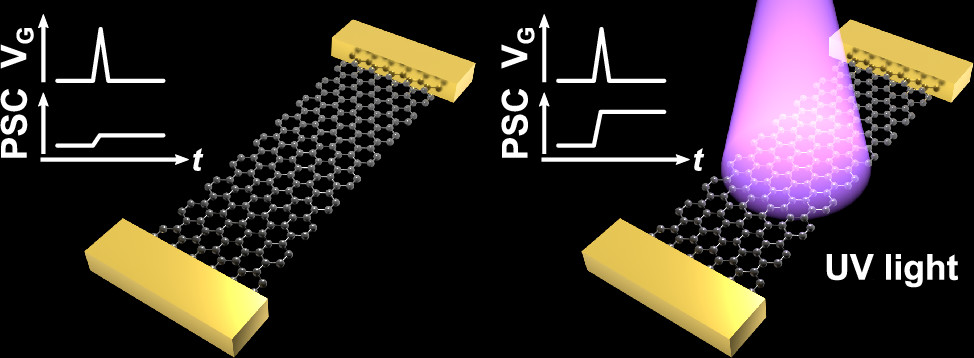
Researchers at @HebrewU have demonstrated how the one atom thick material graphene can be implemented as a neuromorphic transistor. The device emulates the behaviour of a biological neuron and can be stimulated with UV light or electrically. https://t.co/FoEbUcudQ1 /#PHAR
A paradigm shift in chip scale hybrid photonic-atomic devices. Our new work on the nanoscale membrane like waveguide with alkali vapor cladding has been published in #naturephotonics.
Read all about it here:
https://t.co/pAnUIAr44F
#nanophotonics#waveguides#Rubidium#frequency
Researchers at @HebrewU have demonstrated how the one atom thick material graphene can be implemented as a neuromorphic transistor. The device emulates the behaviour of a biological neuron and can be stimulated with UV light or electrically. https://t.co/2QHqnfeDoe /#PHAR
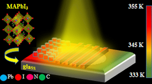
Researchers have used Raman and PL spectroscopy to explore the opto-thermal transport in lithographically patterned MAPbI3 thin films, establishing an operable thermal window for #perovskite metasurfaces with optimal optical efficiencies. @SaswataHalder15
https://t.co/Luwep25usj