From simple current-to-voltage conversion to the heart of high-speed optical links – the evolution of the Transimpedance Amplifier (TIA) 📡⚡
TIAs are the unsung front-end heroes of optical receivers, converting tiny photocurrent from a photodiode into usable voltage. What started as a basic interface has become a critical enabler of performance and efficiency in modern optical systems.
🔹 1970s – The beginning
Early TIAs used op-amp based conversion, sufficient for low data rates. But as speeds increased, the RC time constant at the input (dominated by photodiode capacitance) became a bottleneck.
🔹 2000s – Entering the RF domain
Low-input-impedance topologies (common gate, regulated cascode) emerged. Inductive peaking, multi-stage amps, and impedance matching balanced gain, bandwidth, and noise. The feedback resistor became a key tradeoff node.
🔹 2010s – PAM4 and linearity
Multi-level signaling made distortion a major concern. TIAs began integrating equalization, programmable gain, and adaptive biasing to maintain linearity.
🔹 Device & packaging realities
Higher photodiode responsivity = higher capacitance = lower bandwidth. CMOS offers integration; SiGe and InP deliver speed. Packaging parasitics now dictate high-frequency performance.
🔹 Today – 800G / 1.6T era
Photonic integration and co-packaged optics reduce parasitics. With AI data centers pushing to offload DSP, more functionality is moving into the analog front end – TIAs are absorbing equalization, gain control, and calibration.
🔜 Looking ahead
Optical I/O will move closer to ASICs. Expect ultra-low-power designs, adaptive analog front ends, and heterogeneous integration to define next-gen systems.
From a simple converter to a core system component – the TIA continues to evolve, shaping the future of high-speed, energy-efficient communication.
What trends do you see shaping analog front-end design in the next 5 years? Let me know below 👇
#TransimpedanceAmplifier #OpticalCommunications #HighSpeedDesign #Semiconductors #PAM4 #CoPackagedOptics #AnalogDesign
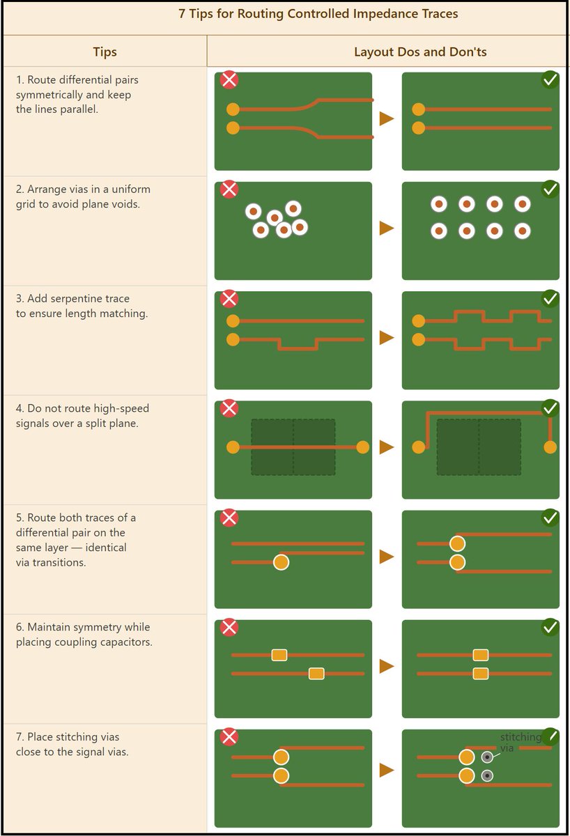
7 Tips for Routing Controlled Impedance Traces 🧵⚡
Controlled impedance routing is one of the most critical aspects of high-speed PCB design.
Small layout mistakes can cause signal integrity problems, reflections, EMI, and unstable communication.
Here are 7 practical tips I always follow when routing controlled impedance traces:
✅ Keep differential pairs symmetrical and parallel
✅ Use uniform via placement to avoid plane discontinuities
✅ Apply proper length matching techniques
✅ Avoid routing over split planes
✅ Keep differential pairs on the same layer whenever possible
✅ Maintain symmetry around coupling capacitors
✅ Add stitching vias close to signal transitions
Good PCB design isn’t just about making connections — it’s about ensuring signal quality and reliability across the entire system.
Which of these rules do you consider the most important in your PCB layouts? 👇
#PCBDesign #HardwareDesign #ElectronicsEngineering #AltiumDesigner #SignalIntegrity #HighSpeedDesign #EmbeddedSystems #Electronics #PCBlayout #Engineering
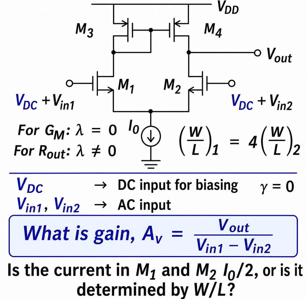
Analog Circuit Design Interview Question
Consider a 5-transistor OTA. The DC voltage at the gate terminals of M1 and M2 is the same. M1 has 4 times the W/L ratio of M2.
Derive the single-ended differential gain Ad = vout / vid = vout / (Vin1 - Vin2) in terms of transistor parameters and the biasing current.
Will the biasing current be equally divided between M1 and M2 regardless of their W/L ratio, or will it depend on W/L?
Share your answers and reasoning below.
#AnalogCircuits #OTA #InterviewPrep #Engineering
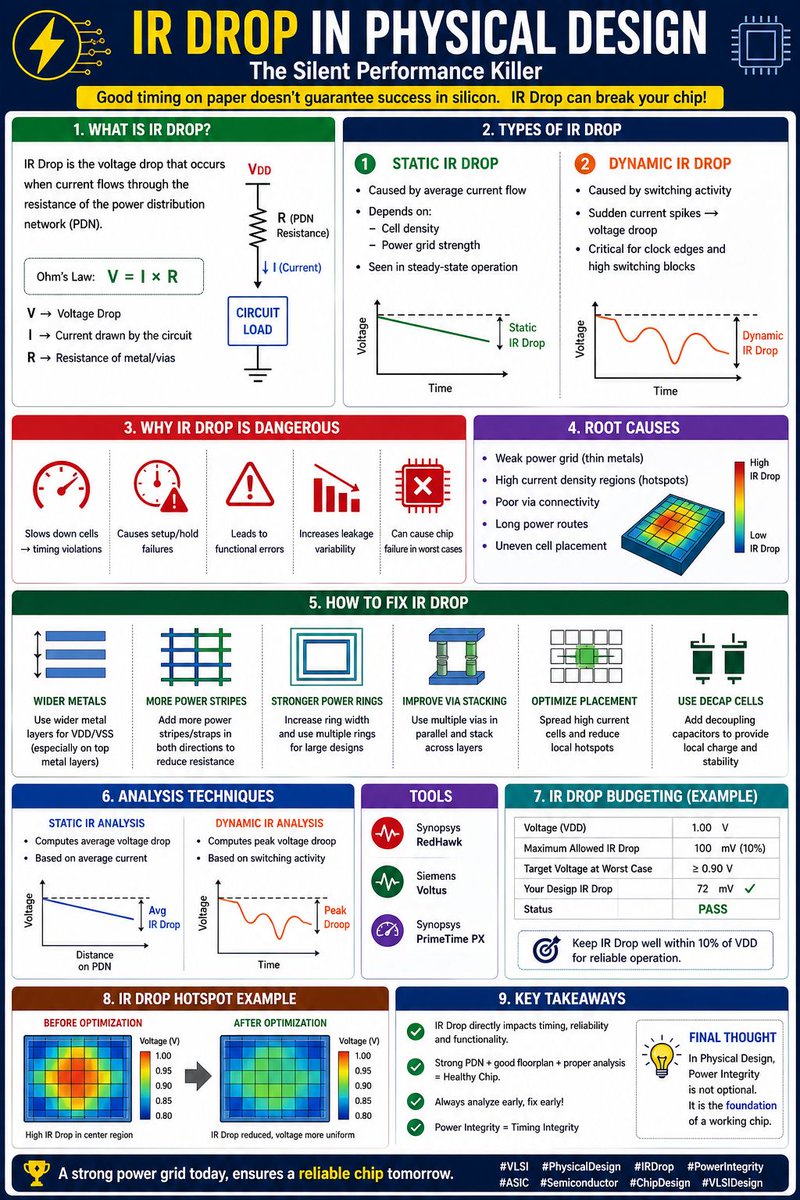
IR Drop in Physical Design – The Silent Performance Killer ⚡
Your timing report looks clean. But if IR Drop isn’t managed, the chip can still fail in silicon.
In VLSI Physical Design, power integrity is just as critical as timing closure.
Let’s break it down 👇
What is IR Drop?
A voltage drop caused by current flowing through the resistance of the power delivery network (PDN).
📐 Based on Ohm’s Law: V = I × R
I = Current drawn by the circuit
R = Resistance of metals / vias
Types of IR Drop
🔹 Static IR Drop
Due to average current flow. Depends on cell density and power grid strength. Seen during steady‑state operation.
🔹 Dynamic IR Drop
Caused by switching activity. Sudden current spikes → voltage droop. Critical near clock edges and high‑switching blocks.
Why IR Drop is Dangerous
❌ Slows down cells → timing violations
❌ Setup / hold failures
❌ Functional errors
❌ Increased leakage variability
❌ Chip failure in worst cases
Root Causes
Weak power grid (thin metals)
High current density regions
Poor via connectivity
Long power routes
Uneven cell placement
How to Fix IR Drop 🛠️
✅ Use wider metal layers for VDD/VSS
✅ Add more power stripes / straps
✅ Strengthen power rings
✅ Improve via stacking
✅ Optimize cell placement (reduce hotspots)
✅ Use decap cells for voltage stability
Analysis Techniques
📊 Static IR Analysis → Average voltage drop
📈 Dynamic IR Analysis → Peak voltage droop
Tools: RedHawk, Voltus, PrimeTime PX
Key Insight
Even a small voltage drop can:
Increase delay
Break timing
Impact reliability
Final Thought
In Physical Design: Power Integrity = Timing Integrity
Ignoring IR Drop is like building a highway without checking the fuel supply — eventually, everything stops.
#VLSI #PhysicalDesign #IRDrop #PowerIntegrity #ASIC #Semiconductor #ChipDesign #VLSIDesign
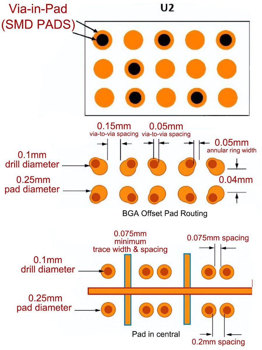
Recently, during a BGA via‑in‑pad discussion, I received a few recurring questions:
◼ Can a non‑conductive epoxy‑filled via‑in‑pad eliminate a via stub?
◼ How do vias affect thermal performance in high‑current nets?
◼ Are copper‑filled vias the same as conductive‑epoxy‑filled vias?
These often get grouped together, but only the first is truly specific to via‑in‑pad. The other two are general via design considerations that frequently come up in BGA routing.
So let’s clarify what via‑in‑pad actually means — and what it doesn’t.
⚪ What Via‑in‑Pad Really Means
In fine‑pitch BGA routing, vias are sometimes placed directly inside pads because there’s no space between pads.
But via‑in‑pad is not simply “a via drawn on a pad.”
If a standard via is placed in a BGA pad, solder can wick into the hole during reflow, causing unreliable joints.
That’s why a true via‑in‑pad requires filling and capping (IPC‑4761 Type VII) to create a flat, solderable surface.
⚪ Real‑World Layout Options
Centered microvias
Offset (dogbone‑style) via‑in‑pad
Blind via‑in‑pad (to control stub length)
Each choice trades off routing density, cost, and manufacturing complexity.
⚪ Signal Integrity – The Via‑in‑Pad‑Specific Question
When a via‑in‑pad is properly filled and capped, it no longer behaves like an open via stub from a signal integrity perspective.
That’s why filled via‑in‑pad structures are widely used in high‑speed and RF BGA designs.
⚪ Thermal & Fill Material – Broader Via Considerations
Beyond via‑in‑pad, vias also affect thermal and current performance. Multiple vias, larger drills, and connections to inner planes help spread heat and reduce current density.
Fill material matters:
Copper‑filled vias → excellent current & thermal conduction
Conductive‑epoxy‑filled vias → far less conductive; chosen for planarity or process reasons, not performance
These considerations apply to any via, not just via‑in‑pad.
📌 A DFM Note
Via‑in‑pad is a defined manufacturing process — not a layout shortcut.
Many questions raised in via‑in‑pad discussions are actually about general via behavior. Separating the two avoids confusion and leads to better design and DFM decisions.
“Good design is buildable design.”
What’s your biggest challenge with BGA via‑in‑pad? Let’s discuss below. ⬇️
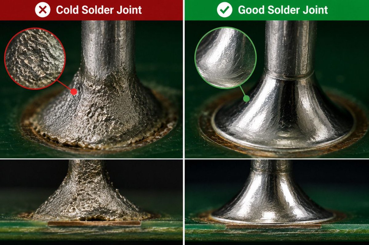
Common PCB defects do not announce themselves until the damage is done. By then, the cost is measured not just in rework hours but in warranty claims, customer trust, and production downtime.
The challenge? Some defects are difficult to identify through visual inspection alone.
A reliable inspection strategy includes:
🔹 Visual Inspection – Identify visible signs of poor wetting or irregular solder joints.
🔹 AOI – Detect visible soldering defects and component placement issues.
🔹 X-Ray Inspection – Evaluate hidden solder joints, particularly those under BGA components.
🔹 Electrical Testing – Verify circuit connectivity and identify functional failures.
👉 Welcome to the discussion. Feel free to share your experience.
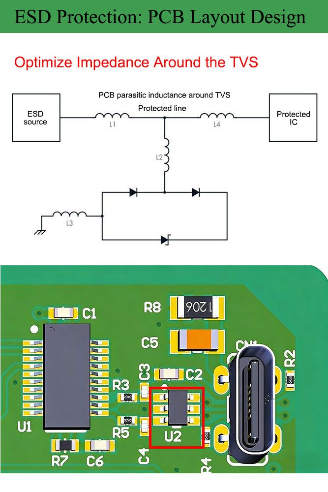
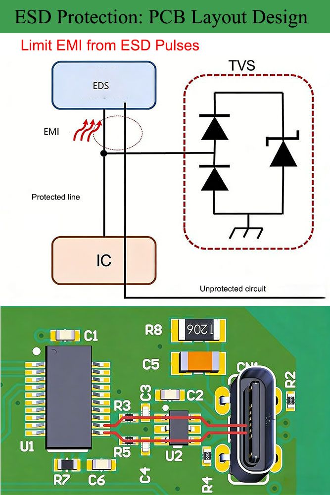
ESD Protection in PCB Layout: 6 Practical Guidelines
ESD can quietly ruin a robust design. Here are several proven layout practices to keep your electronics safe.
🟡 Optimize impedance around the TVS
Every trace has parasitic inductance. In a typical protection path, you’ll find inductance between:
ESD source → TVS
TVS → GND
TVS → protected IC
🔑 Key principle:
Make the impedance between TVS and IC higher than the path from the ESD source to the TVS. This forces the surge current into the protection device — not your IC.
🟡 Limit EMI from ESD pulses
Fast voltage transitions from ESD can radiate strong EMI. Nearby traces act like antennas or capacitive couplers, spreading energy into other circuits.
✅ How to reduce coupling:
Isolate protection areas from sensitive signals
Don’t route unprotected signals near ESD paths
Use short, direct traces
Avoid sharp routing angles
🟡 Use vias carefully
Vias add inductance. If your signal path from the ESD source to the IC includes vias before the TVS, some ESD energy may bypass protection.
👉 Best practice:
Keep the ESD source and TVS on the same layer. Avoid vias between them — ensure the ESD current hits the TVS first.
🟡 Place the ESD suppressor properly
Position the TVS as close as possible to the ESD entry point (USB, HDMI, Ethernet, external cables). The goal: intercept the surge immediately.
📌 Golden rule:
Connector → TVS → protected IC
Order is everything.
🟡 Avoid vias between ESD source and suppressor (even when unavoidable)
If vias can’t be avoided, be extra careful. Wrong routing can steer ESD current toward the IC before reaching the TVS.
A better compromise:
Keep the TVS directly in the signal path
Place the protected circuit downstream of the suppressor
🟡 Provide proper grounding
A TVS is only as good as its ground connection. High-impedance ground kills clamping performance.
✅ Recommended:
Connect TVS directly to the ground plane
Use multiple ground vias
Keep the ground path short and wide
This creates a low-impedance path for safe ESD dissipation.
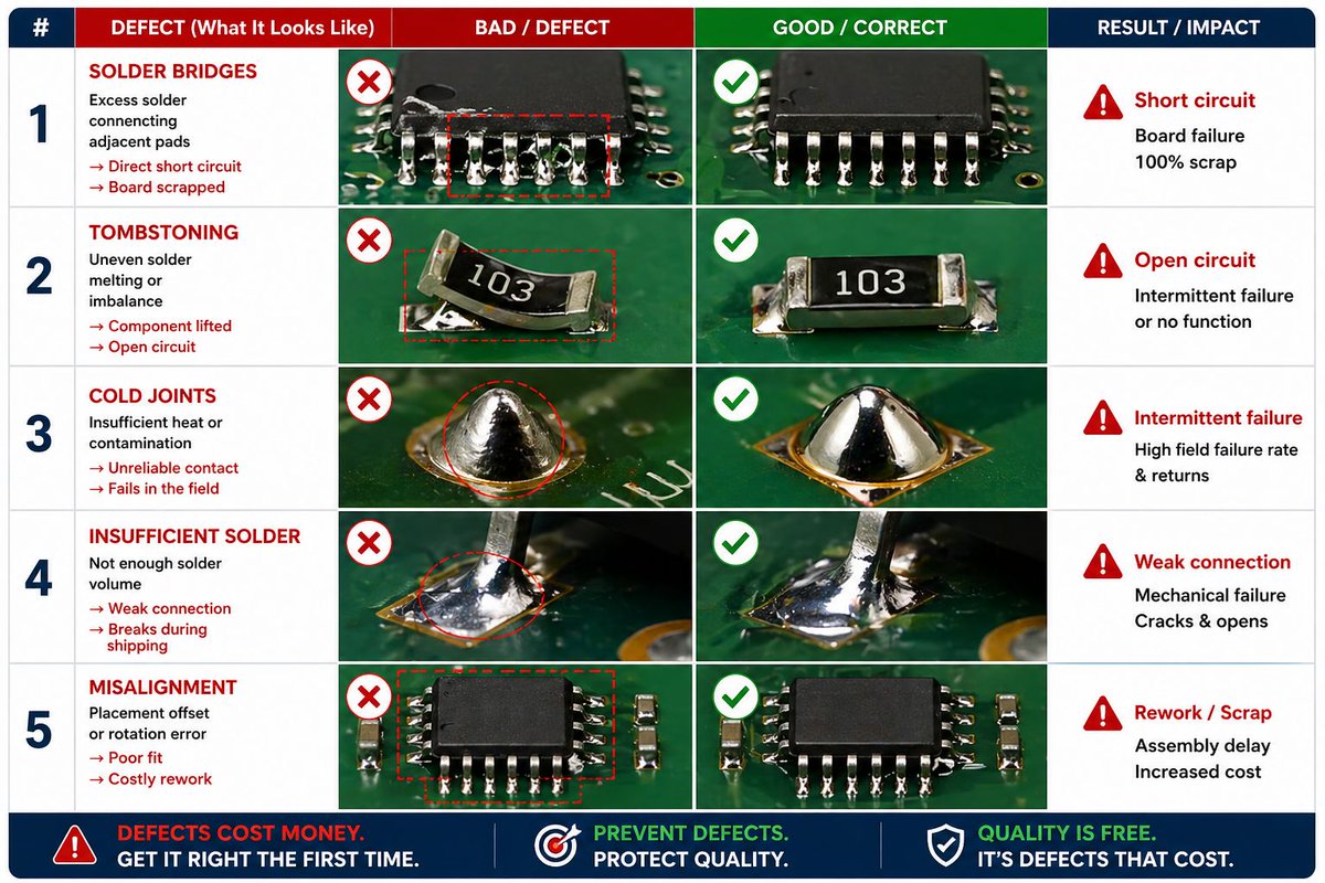
Top 5 SMT Defects That Cost You $10,000+ (And How to Avoid Them)
Most people assume SMT is fully automated.
❌ It’s not.
In fact, that misconception costs the electronics industry $10 billion every year.
Even with million-dollar high-speed pick-and-place machines and advanced reflow ovens, defects still happen daily.
The worst part? 80% are completely preventable.
And they almost always trace back to one of these 5 common defects:
🔹 Solder bridges → Direct short circuit = entire board scrapped
🔹 Tombstoning → One side of component lifts = open circuit
🔹 Cold joints → Unreliable contact = field failures
🔹 Insufficient solder → Weak connection = breaks during shipping
🔹 Misalignment → Placement errors = costly rework
I’ve seen each of these cost a company $50,000+ in a single batch.
⚠️ The real insight?
None of these were random accidents.
They all came down to the same 3 tiny process variations — ones that 90% of EMS factories ignore to save 10 minutes a day.
And those 10 minutes often lead to $10,000+ in rework:
• Bad stencil design
• Uncalibrated reflow temperature profiles
• Outdated placement machine calibration
In EMS, a 0.01mm mistake in stencil design can become a $100,000 loss in production.
✅ How we eliminate these defects before they happen
This isn't rocket science. It's just doing the basics right — the basics that 90% of factories skip to save 10 minutes.
❌ Typical factory✅ What we do
One-size-fits-all stencilsCustom stencils for every component
Calibrate rarelyCalibrate weekly + verify per batch
Occasional placement checksDaily placement accuracy checks
No FAI100% First Article Inspection (FAI)
AOI onlyAOI + X-ray for all hidden joints
Manufacturing isn't just about machines. It's about control, precision, and refusing to cut corners.
If you're an engineer, mastering these basics will save you more time, money, and headaches than any new machine ever will.
👇 Which of these defects has given you the worst headache? Drop a comment below.
#SMT #PCBA #ElectronicsManufacturing #QualityControl #LeanManufacturing
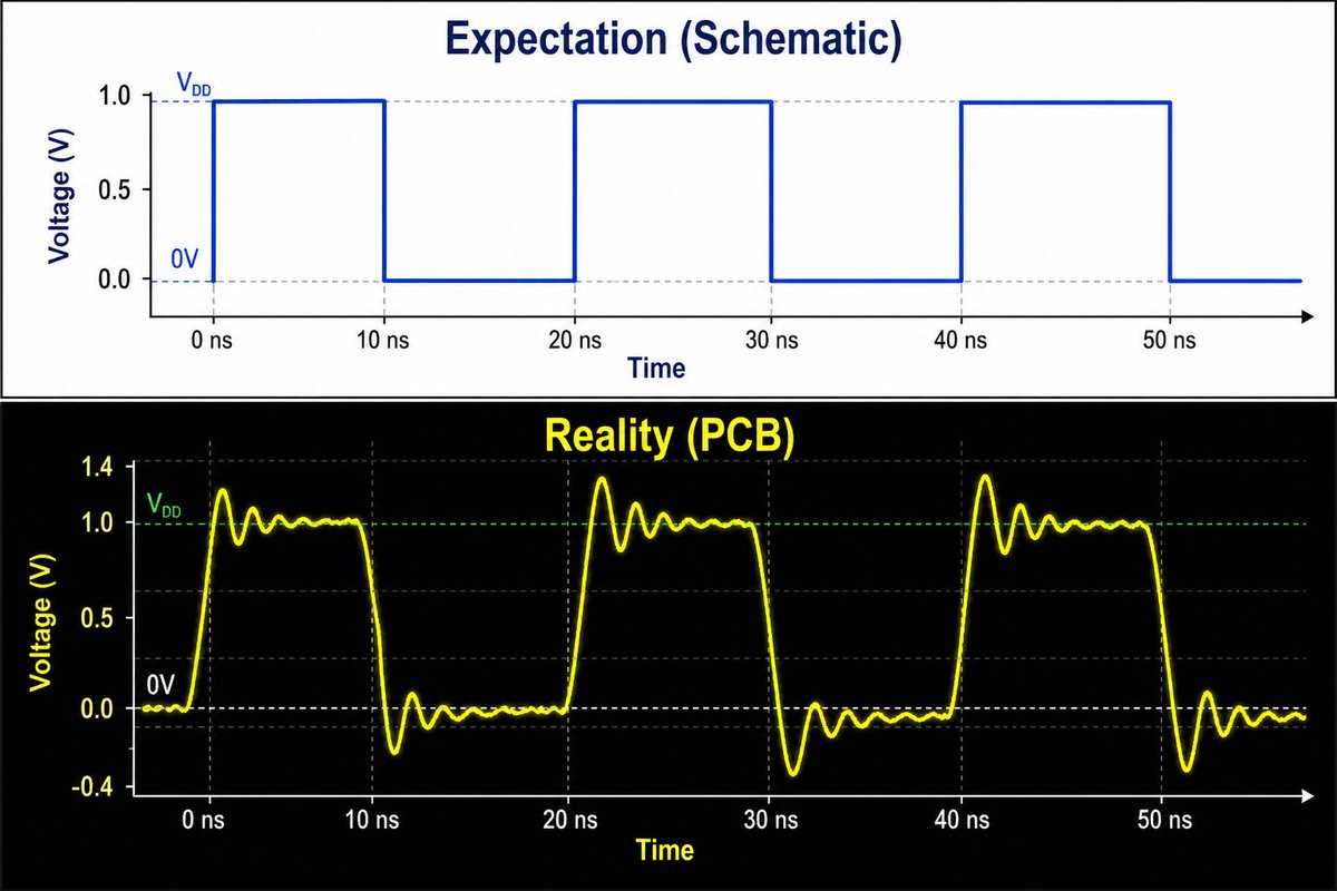
The myth of the "digital" signal (spoiler: it's all analog). 📡
Here's a reality check for digital designers: pure digital signals don't actually exist in the physical world. 🤯
On a schematic, a net looks like a clean, ideal line passing neat 1s and 0s. But the moment you route that net onto a real PCB—with sub-nanosecond rise times—you've left the digital domain behind.
You're now deep in the world of high-frequency analog electromagnetics.
✅ Every trace becomes a transmission line.
✅ Every via behaves like an inductor and a capacitor.
That's where Signal Integrity (SI) comes in.
SI is the art of ensuring that the "1" your transmitter sends still looks like a "1" when it reaches the receiver—despite all the analog physics (reflections, crosstalk, loss) trying to distort it along the way.
To build reliable, high-speed boards, we have to stop thinking purely in 1s and 0s. Instead, think voltage, current, and impedance over time.
💬 What was your first "welcome to the analog world" moment as a digital designer? Drop your story below!
#SignalIntegrity #PCBDesign #HardwareEngineering #HighSpeedDesign #Electronics
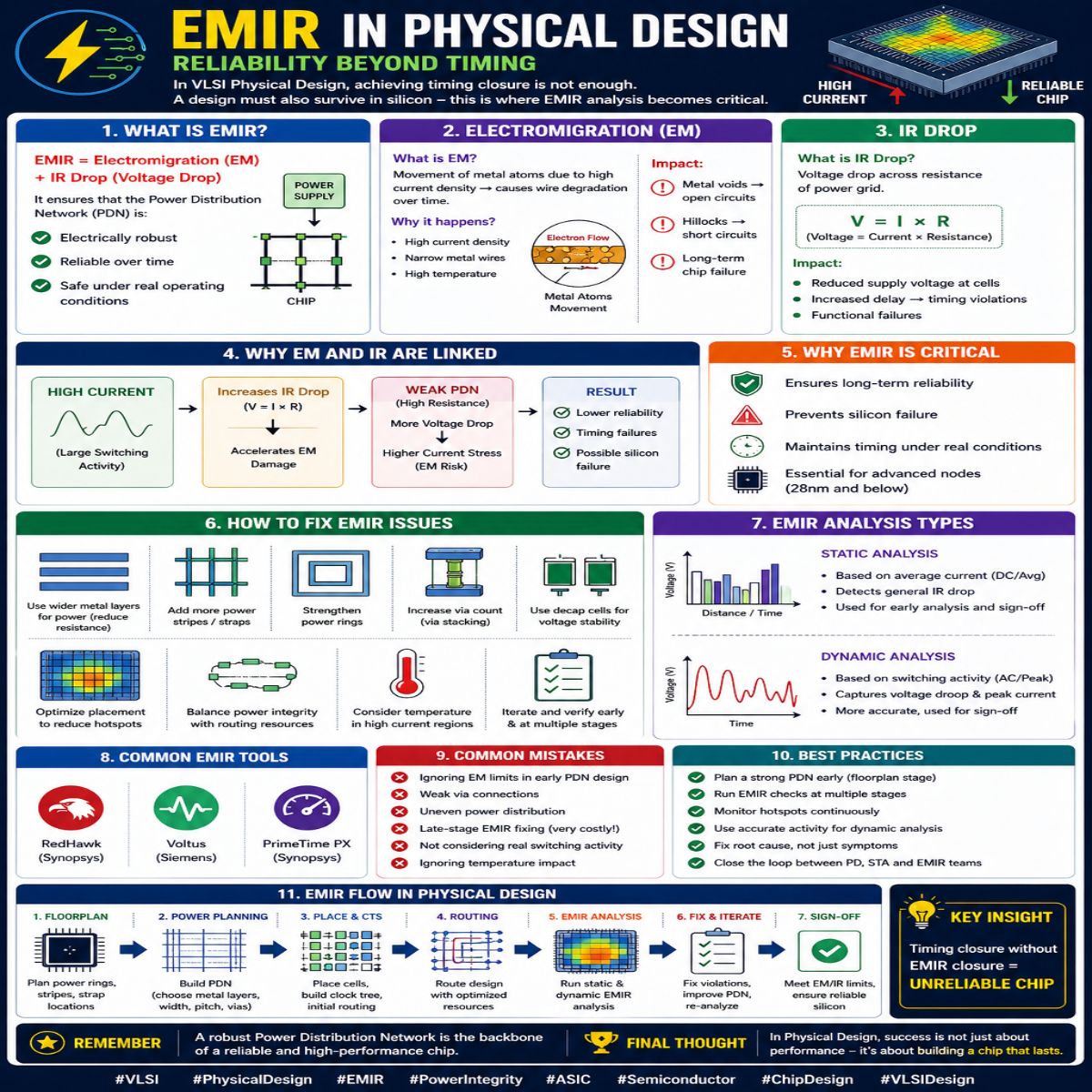
EMIR in Physical Design: Why Reliability Matters Beyond Timing
In VLSI Physical Design, timing closure alone doesn’t guarantee a working chip.
The real challenge? Making sure the design survives in silicon.
That’s where EMIR (Electromigration & IR Drop) comes in.
What is EMIR?
EMIR = Electromigration (EM) + IR Drop (Voltage Drop)
It ensures the power distribution network (PDN) is:
⚡ Electrically robust
⏳ Reliable over time
✅ Safe under real operating conditions
1. Electromigration (EM)
Movement of metal atoms due to high current density → wire degradation over time.
🔍 Why? High current density + narrow wires + high temperature
⚠️ Impact:
Metal voids → open circuits
Hillocks → short circuits
Long-term chip failure
2. IR Drop
Voltage drop across power grid resistance (V = I × R)
⚠️ Impact:
Reduced supply voltage at cells
Increased delay → timing violations
Functional failures
Why EM and IR are linked
🔗 High current → higher IR drop + faster EM damage
🔗 Weak PDN → more resistance → more voltage drop → higher EM risk
Why EMIR is critical
✅ Ensures long-term reliability
✅ Prevents silicon failure
✅ Maintains timing under real conditions
✅ Essential for advanced nodes (28nm & below)
How to fix EMIR issues
Use wider metal layers for power
Add more power stripes / straps
Strengthen power rings
Increase via count (via stacking)
Add decap cells for voltage stability
Optimize placement to reduce hotspots
Analysis types
📊 Static – average current, general IR drop
⚡ Dynamic – switching activity, voltage droop & peak current
Common tools
RedHawk | Voltus | PrimeTime PX
Common mistakes
❌ Ignoring EM limits in early PDN design
❌ Weak via connections
❌ Uneven power distribution
❌ Fixing EMIR too late (costly!)
Best practices
✅ Plan strong PDN early (floorplan stage)
✅ Run EMIR checks at multiple stages
✅ Monitor hotspots continuously
✅ Balance power integrity with routing resources
Key takeaway
🎯 Timing closure without EMIR closure = unreliable chip.
In physical design, success isn’t just about performance — it’s about building a chip that lasts.
#VLSI #PhysicalDesign #EMIR #PowerIntegrity #ASIC #Semiconductor #ChipDesign #VLSIDesign
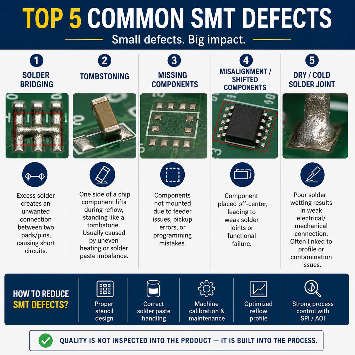
Top 5 Common SMT Defects — and How to Avoid Them 🛠️
In Surface Mount Technology (SMT), small defects can quickly lead to big problems: reduced reliability, higher rework costs, and unhappy customers.
Here are 5 of the most frequent SMT defects seen on production lines — plus practical ways to prevent them.
❗ 1. Solder Bridging
Excess solder creates an unintended connection between two pads or pins → short circuits.
❗ 2. Tombstoning
One side of a chip component lifts during reflow, standing upright like a tombstone. Common causes: uneven heating or solder paste imbalance.
❗ 3. Missing Components
Components aren’t placed due to feeder issues, pickup errors, or programming mistakes.
❗ 4. Misalignment / Shifted Components
Off-center placement leads to weak solder joints or functional failures.
❗ 5. Dry / Cold Solder Joint
Poor solder wetting results in weak electrical and mechanical connections — often linked to reflow profile issues or contamination.
✅ How to reduce SMT defects:
Optimize stencil design
Handle solder paste correctly
Perform regular machine calibration & maintenance
Fine-tune your reflow profile
Use strong process control (SPI & AOI)
💡 Quality isn’t inspected into a product — it’s built into the process.
What’s the most common SMT defect you see on your line? Let me know in the comments ⬇️
#SMT #ElectronicsManufacturing #PCBAssembly #QualityControl #ManufacturingExcellence #LeanManufacturing #ProcessImprovement #AOI #SPI #EMS
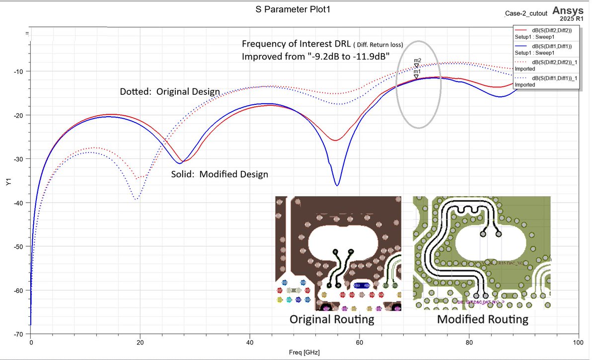
🚀 Is straight signal routing always the best choice?
Conventional wisdom says yes, but our latest simulation work tells a different story.
While simulating an ASIC package (with a #224Gbps SERDES side and a #140Gbaud line‑side), we uncovered something unexpected.
The PCB routing engineer did an excellent job on a short‑length trace – visually, everything looked fine. However, simulations revealed that the required return loss wasn't being met, even after several optimization attempts.
Then we tried an out‑of‑the‑box concept. The result? A dramatic improvement in return loss.
💡 Takeaway: In high‑speed design, assumptions can be limiting. Sometimes the best solution isn't the most obvious one.
Have you ever challenged a "rule of thumb" and found a better path? Let's discuss below.
#SignalIntegrity #HighSpeedDesign #PCBDesign #SERDES #EngineeringInnovation
🔌 Simple R-C Model for MOSFET Switching Loss Calculations
In power electronics design, accurate switching loss estimation is critical for efficiency and thermal reliability.
Before diving into complex non-linear models, a first‑order R‑C approximation based on gate charge behavior offers a quick, practical engineering check.
How it works (during turn‑on):
• Gate resistance (Rg) + input capacitance Ciss (= Cgs + Cgd) → before Miller plateau
• Gate resistance (Rg) + Miller capacitance Cgd → after Miller plateau
Switching intervals are derived from exponential charging equations:
➡️ Drain current rise/fall happens when gate‑source voltage reaches Vth
➡️ Drain‑source voltage fall/rise occurs during the Miller plateau (Vgp)
Switching loss formula:
MOSFET Switching Loss = 0.5 × (t_on + t_off) × Vds × Id × f_sw
For a conservative design, I use maximum Ciss and Cgd from the datasheet (not typical values).
This gives:
✅ Worst‑case switching time
✅ Higher (safer) loss prediction
✅ Better thermal margin under real‑world variations
Why this matters:
Datasheet capacitances are voltage‑dependent and non‑linear – measured under specific test conditions.
Using maximum values simplifies analysis without underestimating losses.
Trade‑off to keep in mind:
📈 Max Ciss/Cgd → Conservative, safer → Overestimates losses
📉 Typical Ciss/Cgd → Closer to reality → Underestimates losses
Bottom line:
This method has been especially useful for quickly validating switching behavior before moving to detailed simulations or hardware testing.
If you design power converters, motor drives, or high‑frequency switching systems with MOSFETs, this approach saves time while keeping loss margins safe.
#PowerElectronics #MOSFET #SwitchingLoss #GateDrive #AnalogDesign #HardwareEngineering #ElectronicsDesign #PowerConverters #DCDCConverters #DCACConverters #Semiconductor #EnergyEfficiency #MotorDrives
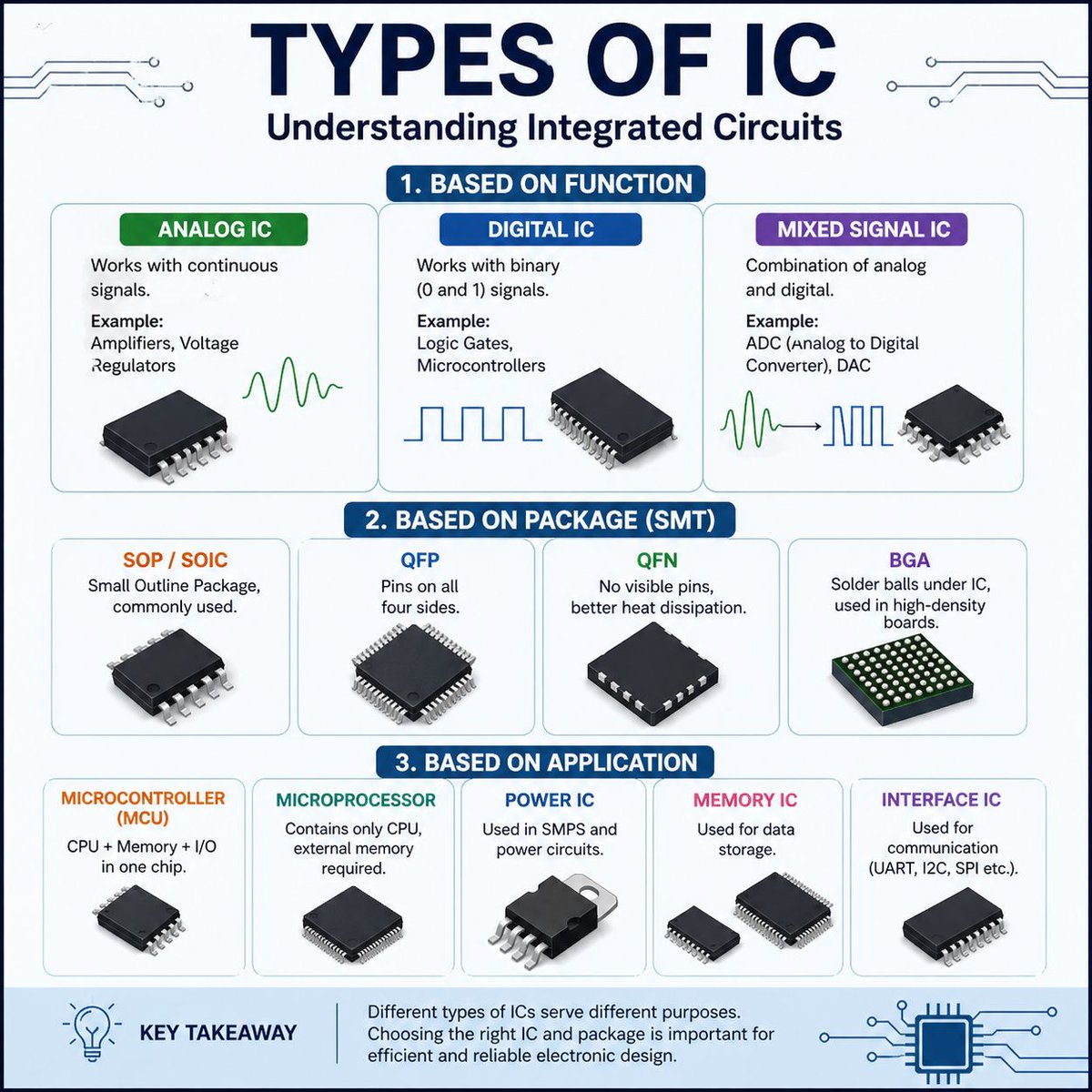
🔹 Understanding IC Types: A Simple Guide for Engineers & Beginners 🔹
Integrated Circuits (ICs) are the brains behind nearly every electronic system. Whether you're just starting out or need a quick refresher, here’s a clear breakdown of IC types, packages, and applications 👇
✅ By Signal Type
🔸 Analog IC – Processes continuous signals (sound, temp, voltage)
👉 Examples: Amplifiers, Voltage Regulators
🔸 Digital IC – Works with binary (0 & 1) signals
👉 Examples: Logic Gates, Microcontrollers
🔸 Mixed-Signal IC – Combines analog & digital functions
👉 Examples: ADC, DAC
✅ By Package (Surface Mount)
📦 SOP / SOIC – Compact & widely used
📦 QFP – Pins on all four sides
📦 QFN – No visible pins, excellent thermal performance
📦 BGA – Solder balls underneath, ideal for high-density boards
✅ By Application
⚙️ Microcontroller (MCU) – CPU + memory + I/O in one chip
⚙️ Power IC – Key in SMPS & power management
⚙️ Memory IC – RAM, ROM, Flash
⚙️ Interface IC – Enables UART, I2C, SPI communication
💡 SMT Insight
Handling diverse IC packages—especially QFN and BGA—demands high placement accuracy, optimized reflow profiles, and robust inspection methods like AOI and X-ray.
Understanding the Building Blocks of Modern Electronics ⚡
Transistors and capacitors are the unsung heroes behind every electronic system – from smartphones to advanced computing devices.
This visual guide breaks down the key types of transistors and capacitors, including their symbol structures, arrow directions, and – most importantly – real-world applications.
What you’ll learn:
🔹 The differences between BJT, MOSFET, and JFET transistors
🔹 How arrow direction defines current flow and device behavior
🔹 Key capacitor types – ceramic, electrolytic, film, and supercapacitors
🔹 Practical applications in power systems, signal processing, filtering, and energy storage
💡 Whether you're an engineering student, electronics enthusiast, or industry professional, this infographic simplifies complex concepts into an easy-to-understand format.
Master the fundamentals. Build the future. 🚀
#Electronics #Engineering #ElectricalEngineering #Transistors #Capacitors #TechEducation #STEM #Innovation #CircuitDesign