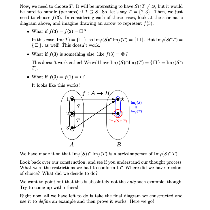
"Everything You Always Wanted to Know About Mathematics" is a freely available, almost 700-page book that provides a broad introduction to abstract mathematics and mathematical reasoning.
It starts with a fundamental question, "What is mathematics?", and develops the tools needed to think and write mathematically. It covers mathematical induction, sets, logic, functions, relations, modular arithmetic, combinatorics, proof techniques, and much more.
I find it a particularly interesting and substantial resource, worth keeping as a reference and consulting whenever needed.
https://t.co/dU5UjXWgfo
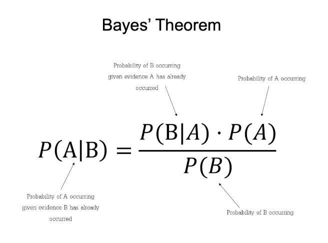
Bayes' Theorem is a fundamental concept in data science.
But it took me 2 years to understand its importance.
In 2 minutes, I'll share my best findings over the last 2 years exploring Bayesian Statistics. Let's go.
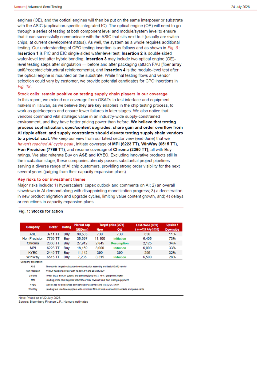
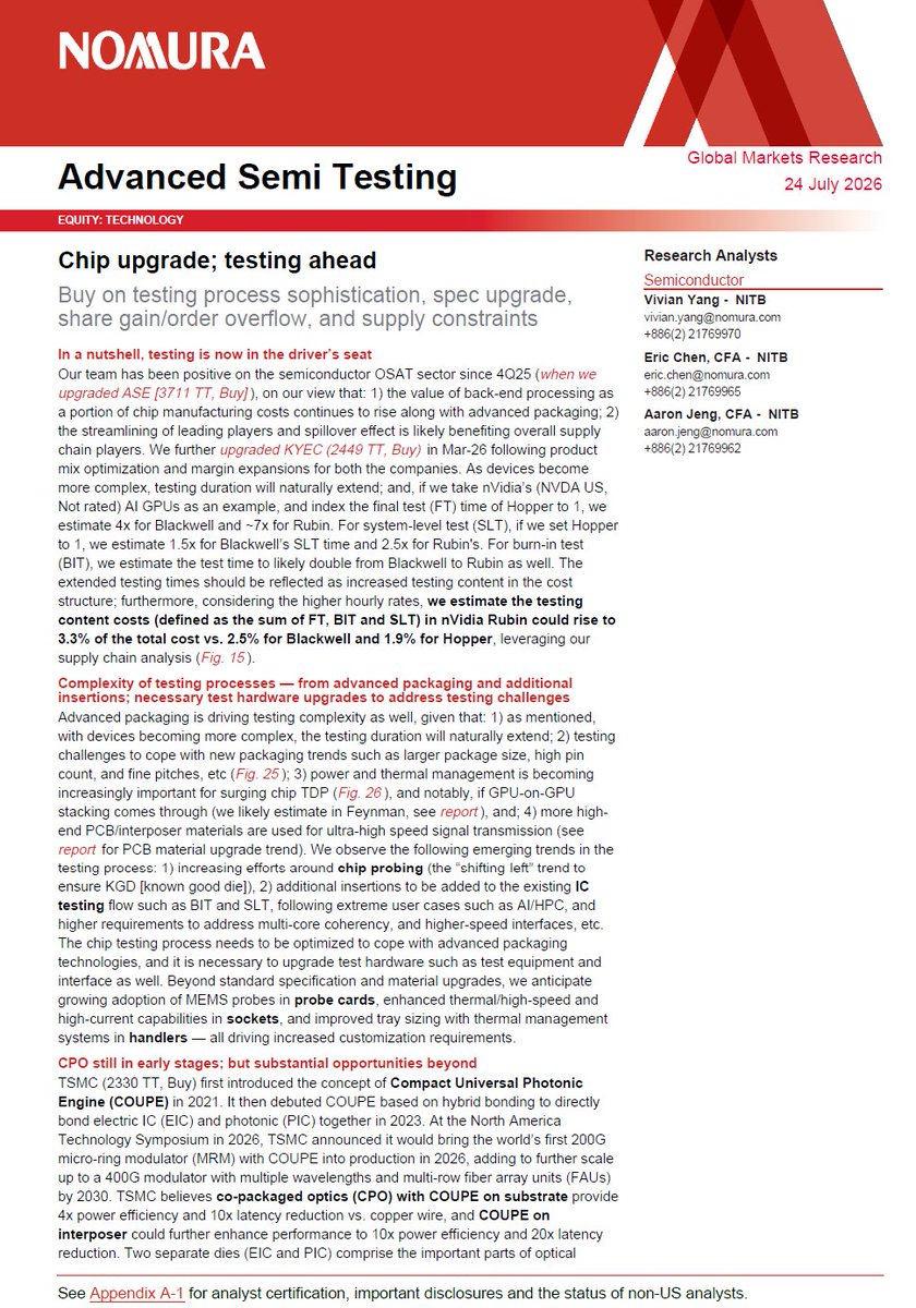
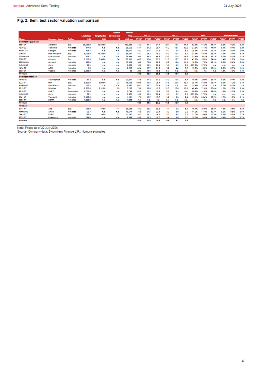
Nomura's report reinforces what we believe is one of the most underappreciated structural shifts taking place across the semiconductor industry today, namely that testing is no longer a low-value manufacturing step performed at the end of production, but is rapidly evolving into one of the most critical value-added processes within the entire AI hardware supply chain, because as chips become exponentially more complex through chiplets, stacked HBM, advanced packaging, silicon photonics and eventually co-packaged optics (CPO), the economic cost of failure rises disproportionately, making every additional dollar spent on testing significantly more valuable than it was during previous semiconductor cycles.
The market has understandably spent the past two years focusing almost exclusively on GPU designers, HBM suppliers and advanced packaging companies, yet what this report demonstrates is that testing is quietly becoming the next bottleneck, because increasingly sophisticated AI accelerators cannot simply be manufactured, they must be validated repeatedly throughout the production process to ensure every component performs flawlessly before being assembled into AI systems that may ultimately be worth several million dollars each, effectively transforming testing from a manufacturing support function into an essential yield protection mechanism.
Historically, testing was largely viewed as a necessary manufacturing expense whose primary objective was to filter out defective chips before shipment, but AI has fundamentally altered that equation because testing today is increasingly about protecting economic value rather than merely measuring quality, and when a single package contains multiple GPU chiplets, twelve stacks of HBM, advanced substrates, hybrid bonding interfaces, silicon photonic engines and increasingly expensive packaging materials, discovering a defect late in the production process can destroy vastly more value than in previous semiconductor generations.
That is precisely why Nomura estimates testing content continues to increase materially with every GPU generation, using Hopper as the baseline, where final testing time increases approximately fourfold for Blackwell and roughly sevenfold for Rubin, while system-level testing rises approximately 1.5 times for Blackwell and 2.5 times for Rubin, with burn-in testing roughly doubling, resulting in testing content increasing from approximately 1.9% of total GPU cost for Hopper to 2.5% for Blackwell and approximately 3.3% for Rubin, a progression that may appear modest when expressed as percentages but becomes extraordinarily meaningful when applied to AI systems whose selling prices continue rising dramatically.
Perhaps the most important observation in the report is not simply that testing content is increasing, but that testing itself is migrating earlier throughout the manufacturing process, effectively shifting from a single inspection performed after fabrication into a continuous validation framework that begins at wafer probing, continues through known-good-die verification, hybrid bonding validation, package testing, burn-in qualification and ultimately system-level testing before deployment inside hyperscale AI clusters, meaning the industry is increasingly adopting multiple quality gates rather than relying on one final inspection at the end of production.
This shift has enormous implications for the supply chain because every additional testing insertion creates incremental demand for specialized equipment, probe cards, sockets, handlers, MEMS probes, thermal management systems and high-speed interfaces, thereby expanding the opportunity set well beyond traditional outsourced semiconductor assembly and test companies, which explains why Nomura has broadened its coverage to include interface suppliers and test hardware manufacturers rather than limiting its investment thesis solely to OSAT providers.
Another theme that deserves significantly more attention is the interaction between advanced packaging and testing, because while investors have understandably focused on CoWoS capacity as one of the industry's largest bottlenecks, packaging capacity alone cannot solve the industry's challenges if testing capacity fails to expand at a similar pace, since every additional layer of complexity introduced through chiplets, hybrid bonding, HBM stacking, heterogeneous integration and silicon photonics simultaneously increases the probability that expensive failures will occur after substantial value has already been added to the product, making testing increasingly indispensable as AI hardware becomes more sophisticated.
The discussion surrounding co-packaged optics is equally compelling because most investors naturally associate CPO with optical component suppliers, whereas Nomura correctly argues that the real opportunity extends much further into the testing ecosystem, given that every optical engine must communicate flawlessly with adjacent ASICs under extremely demanding thermal, electrical and optical conditions while maintaining signal integrity across increasingly complex architectures, thereby introducing entirely new categories of testing that simply did not exist in previous semiconductor generations and creating an additional secular growth driver for testing vendors.
We also agree with Nomura's conclusion that the AI infrastructure cycle remains considerably earlier than many investors assume, because every successive GPU generation is becoming disproportionately more difficult to validate than its predecessor, allowing testing content to grow materially faster than semiconductor unit volumes themselves, which means the industry's next major beneficiaries may not necessarily be the companies designing the chips, but increasingly the companies ensuring those chips actually function reliably inside increasingly expensive AI systems.
Our preferred way to position for this theme is to own the entire testing value chain rather than focusing solely on OSATs, because different parts of the ecosystem benefit from different stages of the testing process. ASE (3711 TT) remains our highest-conviction OSAT exposure given its scale, broad customer base and dominant position across advanced packaging and testing. Hon Precision (7769 TT) stands out as one of the most attractive pure-play beneficiaries of final testing and system-level testing, areas where AI complexity is expanding the fastest. WinWay (6515 TT) offers differentiated exposure through sockets and probe cards, which should experience rising content per AI accelerator as electrical and thermal requirements become increasingly demanding. MPI (6223 TT) is well positioned through wafer probing, benefiting directly from the industry's shift toward earlier testing insertions and known-good-die validation. KYEC (2449 TT) remains an attractive second OSAT exposure with meaningful leverage to AI testing demand, while Chroma (2360 TT) provides exposure to automated testing equipment, allowing investors to participate in the hardware upgrade cycle required to support increasingly sophisticated AI devices.
Ultimately, we believe semiconductor testing has quietly transitioned from a manufacturing support function into one of the industry's most valuable strategic chokepoints, and just as HBM suppliers, advanced packaging companies and foundries have enjoyed structurally stronger pricing power because they occupy indispensable positions within the AI value chain, testing vendors increasingly appear poised to achieve similar economics as AI hardware becomes more heterogeneous, more thermally demanding, more optically integrated and substantially more expensive to manufacture, making testing one of the highest-conviction secular investment opportunities across the broader semiconductor ecosystem.