The SOI Industry Consortium is a group of leading companies from the electronics industry with the mission of accelerating silicon-on-insulator (SOI) innovation
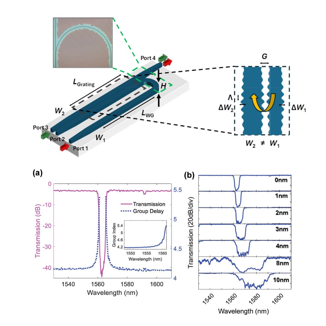
This work represents efficient #SOI devices for temporal pulse compression, achieving up to 3.6× compression and realizing a mass-manufacturable, wafer-scale #CMOS foundry process.
Read: https://t.co/TQma2pvkFq
#photonics#innovation
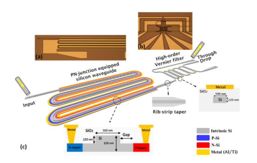
This work demonstrates a scalable design paradigm for integrated digital photonic computing chips on a #SOI platform, achieving a 200% increase in on-chip functional density.
Read: https://t.co/t1mepAxUhF
#photonics#research#tech
This work demonstrates the scalable heterogeneous integration of #GaN HEMTs using a micro-transfer printing process. The technique achieved a high transfer success rate with limited device degradation.
Read: https://t.co/Cc2sJHkVVC
#research#semiconductor
Focusing on angled finger configurations adhering to a 10 µm #SOI platform, this study shows that angled fingers significantly enhance both force intensity and travel range within a compact footprint.
Read: https://t.co/I3qap7LqmU
#photonics#tech#research
This research demonstrates that inverse-designed silicon nitride photonic devices can achieve a >1200x footprint reduction, enabling high-density integration for optical communications and quantum applications.
Read: https://t.co/TyXK3fmgH9
#SOI#photonics#research
This study proposes a novel, compatible, and efficient selective protection process using a magnesium fluoride thin film to prevent waveguide collapse during hydrofluoric acid (HF) release on the #SOI platform.
Read: https://t.co/r4dA6gtwLn
#photonics#research
This work presents a fully integrated silicon photonic wavelength converter on an #SOI platform, combining efficient four-wave mixing with a widely tunable on-chip filter to achieve high pump suppression.
Read: https://t.co/CSMfSeNQex
#photonics#research
NTT Research, in collaboration with Cornell and Stanford, demonstrated the world’s first programmable nonlinear photonic waveguide.
Read more: https://t.co/Id0e1KLsnw
#photonics#innovation#computing
Researchers demonstrates a method to control active interface trap states in an AlGaN/GaN transistor structure by tuning the stress and layer configuration of the SiNx passivation layer.
Read: https://t.co/9KJBdqufb4
#GaN#HEMT#research
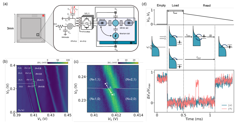
This work demonstrates single-shot spin readout with visibilities exceeding 90% in addressable quantum dot devices fabricated using 22 nm #FDSOI technology. This achievement is a key step towards realizing highly scalable and integrated spin qubits.
Read: https://t.co/FG9pHScbXi
Researchers have demonstrated a high-performance, single-mode hybrid integrated laser built on a 3 µm #SOI platform. This optimized design successfully combines a waveguide Bragg grating with a SOA chip.
Read: https://t.co/qi7Bbibf49
#photonics#tech#research
This research proposes a universal architecture for a bidirectional protection switch designed for monolithic integration in high-voltage silicon-on-insulator (SOI) technology.
Read: https://t.co/RIKrlvbpW9
#SOI#innovation#tech
Embracing the idea of a technological roadmap with multiple parallel paths such as FDSOI and RFSOI to contextualize the value of differing technologies with specific industry applications, says Jamie Schaeffer, VP at @GlobalFoundries.
#Semiconductors#Sillicon
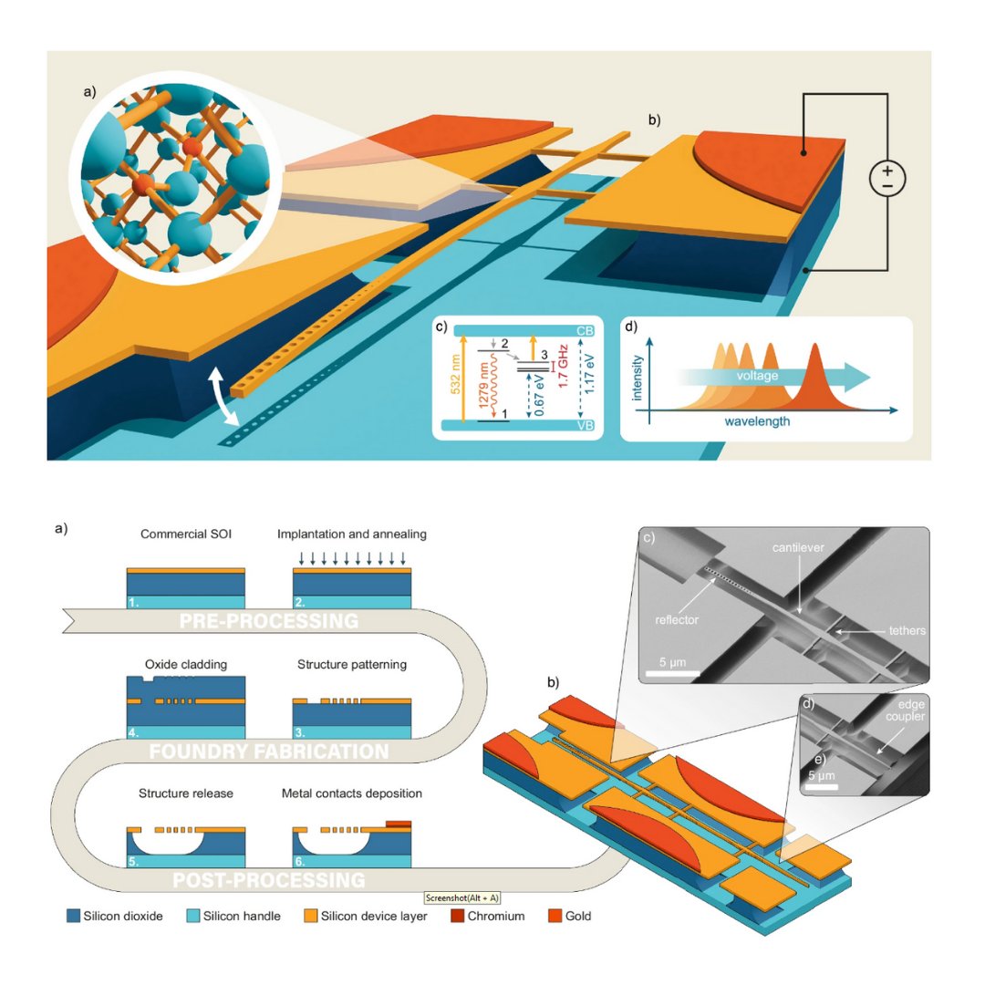
A foundry-made silicon photonics chip uses a #MEMS cantilever to apply strain, precisely tuning the light emission of individual G-center defects for scalable quantum networks.
Read: https://t.co/nL6gL5gthu
#quantum#photonics#SOI
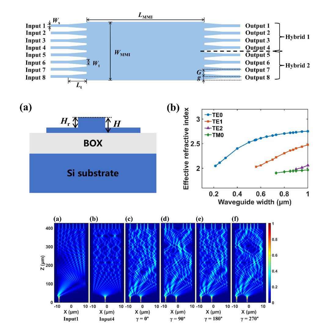
A new dual-channel symmetric optical 90-degree hybrid on a #SOI platform integrates coherent hybrid and signal splitting functions into a compact design. The device reduces insertion loss and layout complexity.
Read: https://t.co/wTLuWmi1rq
#photonics#research
This research demonstrates that silicon-on-insulator (SOI) is more advantageous for compact integration. The findings offer critical insights for integrating these delay lines into photonic circuits for applications.
Read: https://t.co/sEpRd5MXGb
#SOI#research#tech
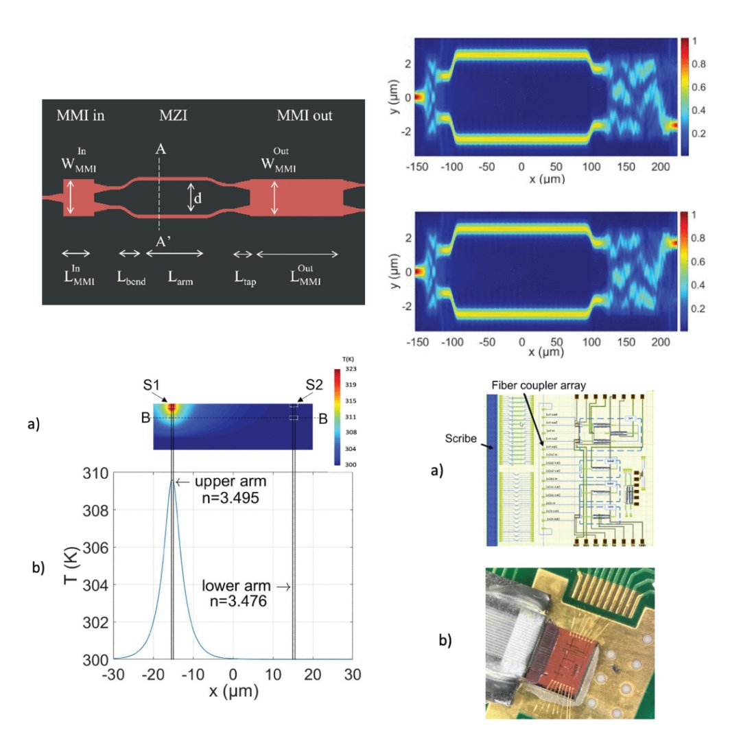
A photonic system was created to remotely power and control a 1x2 thermo-optic switch on a #SOI platform. The system uses power-over-fiber technology to convert light into electricity, which heats and controls the switch.
Read: https://t.co/HyPp4SHkBQ
#photonics#innovation
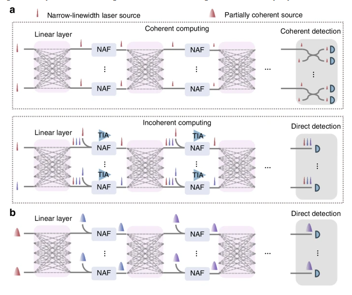
This research presents a monolithically integrated optical neural network with the largest input size and deepest network depth to date, achieving high-accuracy classification while maintaining performance.
Read: https://t.co/9UEugW5wTe
#photonics#AI