Apple did not just get early access to 3 nm. It bought time.When TSMC ramped N3, reports pointed to ~80% yield for Apple’s early chips. Samsung’s first 3 nm GAA reportedly saw ~10–20% yield.On paper, Samsung had the bolder architecture. In production, TSMC had the more usable ramp.That difference ships products.Roadmaps do not ship phones, servers, or accelerators. Yield does. At advanced nodes, yield is where strategy becomes a factory schedule.TSMC’s “boring” choice to stay with FinFET at N3 gave customers what they pay for:- a predictable learning curve - faster defect reduction - enough good die for launch - confidence that supply will exist when promised First-mover advantage at new nodes does not always go to the most advanced architecture. It goes to the company that can make the architecture https://t.co/EKzG6PtH8d’s role is just as strategic: by absorbing early cost and locking initial capacity, it turned yield ramp into product exclusivity.For engineering and operations teams, the pattern is clear: novelty attracts attention; process understanding creates advantage.Where in your world are teams still rewarding the boldest technical choice before proving the most stable one?
At the AI packaging frontier, one word guards the door: Yield.Morgan Stanley (via 36Kr) estimates global CoWoS demand could hit 1M wafers in 2026. Nvidia alone may need ~595k (≈60%), Broadcom 150k, AMD 105k.After the majors “take what they need,” <15% of capacity remains for second-tier AI chipmakers, ASIC vendors, and startups.Advanced packaging is no longer just a technology bottleneck. It is a market-access filter.For smaller AI chip teams, the reality is harsh:Great architecture? Fine. Strong benchmarks? Impressive. Customer interest? Encouraging. No access to high-yield packaging? Please wait.Yield has become a truth serum in semiconductors. It reveals:- Which designs are manufacturable - Which supply chains are trusted - Which companies can scale beyond a slide deck - Which “almost ready” products are still in engineering limbo The uncomfortable lesson: scarce capacity rewards teams that reduce uncertainty fastest.Clearer process models. Better failure reasoning. Earlier constraint mapping. Fewer late-stage https://t.co/YuqYvxRRPZ this level, problem-solving maturity is not a soft https://t.co/ndVsky4Dzt is market https://t.co/DcLJhwqwCm AI chips over the next few years, what becomes the stronger moat: architecture, packaging capacity, or yield discipline?
At 2 nm, a 20-point yield gap is not a footnote.
It is a customer acquisition strategy wearing a cleanroom suit.
Wccftech, citing Taiwan Economic Daily, reported that TSMC’s N2 logic yield had reached roughly 60%, while Samsung’s 2 nm yield was around 40%. The same report says Apple, Nvidia, and AMD had reserved TSMC 2 nm production lines. TSMC’s own site now says N2 entered volume production in Q4 2025.
That gap sounds small until you remember what yield really controls:
cost per good die
available capacity
delivery confidence
top-bin availability
roadmap risk
customer trust
For advanced logic, the customer is rarely buying “nanometers.”
They are buying probability.
Probability that the chip will work.
Probability that volume will ramp.
Probability that the launch date survives contact with physics.
This is where yield becomes strategic. A stronger yield ramp gives premier customers more than lower cost. It gives them architectural confidence. They can plan future CPUs, GPUs, AI accelerators, and mobile SoCs around a process that feels executable.
And for the foundry trailing behind, the problem is painful because “improve yield” is a deceptively simple sentence. Behind it are thousands of interacting variables: lithography, etch, deposition, contamination, thermal budgets, design rules, metrology, packaging, and the occasional gremlin with a PhD.
The spicy part: at 2 nm, technology leadership is less about announcing the node and more about making the node boring enough to trust.
That is the real race.
Who can turn extreme complexity into repeatable manufacturing faster?
At 2 nm, a yield gap is not a detail. It is a moat.
Reports suggest TSMC is above 90% yield at 2 nm, while Samsung struggles to pass 20%. Even if these are only estimates, the signal is clear:
At advanced nodes, yield decides who can play.
Customers do not buy “technology leadership” in theory. They buy confidence:
* Can the supplier deliver volume?
* Will the roadmap survive qualification?
* Are top-bin parts consistently available?
* Will pricing stay rational when demand spikes?
* Can engineering teams resolve excursions fast enough to protect launches?
A beautiful node with weak yield is a sports car that only starts sometimes: impressive specification, stressful ownership.
Yield leadership compounds. Better yield brings more learning cycles, more trust, more design wins, more volume, more data. Low-yield competitors get fewer opportunities to learn at scale. The gap can widen long before the market reacts.
For engineering and quality teams, the lesson is direct: yield is rarely one major issue. It is a network of small frictions, edge conditions, hidden interactions, and untested assumptions.
Teams win when they turn those signals into structured learning before the factory turns them into margin loss.
In advanced manufacturing, the yield dashboard is not only reporting performance.
It is reporting the quality of organizational thinking.
HBM is often discussed like a packaging race.
More layers. Better bonding. Better thermal control. Cleaner stack architecture.
All true.
But the battle may be happening much earlier, in the front-end DRAM process.
Nomad Semi’s HBM analysis makes the point sharply: Samsung is trying to use 1c-nm DRAM for HBM4, while SK Hynix is leaning on a mature 1b-nm process. The spicy part is that “newer node” does not automatically mean “stronger business position.”
In high-volume memory, maturity can beat ambition.
Because HBM yield does not politely wait until final assembly to become painful, every weak die entering the stack becomes a multiplier. A small front-end yield gap becomes a much larger final-stack yield gap once you build 8-high, 12-high, or 16-high products.
That creates the usual factory pain buffet:
• more engineering fire drills
• more qualification anxiety
• more binning pressure
• more capacity consumed by parts that almost work
• more uncomfortable customer conversations
Packaging gets the spotlight because it is visible, exotic, and slightly sci-fi.
Front-end yield gets fewer headlines because it sounds boring.
Which is exactly why it matters.
The winner in HBM may be the company that makes the fewest heroic recoveries later in the flow, because the process was stable enough earlier in the flow.
Advanced manufacturing rewards elegance, but it pays cash for repeatability.
What do you think will matter more in the HBM4 race: aggressive node scaling, or boring-but-beautiful process maturity?
#Semiconductors #HBM #DRAM #Yield #Process #Packaging #Manufacturing #RootCauseAnalysis #AI #Engineering #Semiconductor #PRIZGuru
If a process needs constant babysitting, the control plan is pointing at a design problem.
Weak processes rarely announce themselves. They show up as:
- another inspection
- another review meeting
- another monitor
- another rework loop
- another “temporary” workaround on its 3rd birthday
Each control may be reasonable—even necessary.
But when controls keep accumulating around the same weak spot, the question becomes:
Are we controlling the process, or compensating for one we do not fully understand?
Structured problem solving looks beyond the symptom and asks:
• What function is failing?
• What condition allows it?
• Which interaction creates variation?
• Can we remove the harmful condition instead of supervising it forever?
Every extra control has a carrying cost: training, cycle time, maintenance, false alarms, engineering attention, troubleshooting complexity.
The mature move is process simplification:
- fewer fragile steps
- fewer hidden dependencies
- fewer places where quality relies on someone noticing “the usual weird thing”
The best control is often removing the condition that made control necessary.
What “temporary control” in your factory has clearly become permanent?
#Engineering #Process #ContinuousImprovement #Semiconductor #Semiconductors #PRIZGuru
Eight good dies walk into an HBM stack.
Only two-thirds of the stacks walk out healthy.
That is the brutal math behind high-bandwidth memory.
Nomad Semi’s HBM deep-dive gives a simple example: even with 95% front-end yield, an 8-high stack lands around 66% final yield. Move to 16-high, and the stack yield drops to about 44%.
The formula is innocent.
The business impact is less polite.
Every additional die adds another opportunity for failure: wafer defects, thin-die handling damage, bonding issues, warpage, voids, thermal stress, alignment variation, test escape, repair limits. In 3D memory, yield does not add. It compounds.
That is why bonding technology suddenly becomes a strategic weapon.
SK Hynix’s MR-MUF approach is reported to deliver better thermal dissipation and roughly 20% higher average yield than TC-NCF approaches used by competitors. At HBM scale, that is not a packaging footnote. That is capacity, margin, customer qualification, and AI supply.
This is where many teams feel the pain:
The front-end process looks “good enough.”
The stack still fails.
The root cause hides between process steps, materials, interfaces, and thermal behavior.
Everyone brings data. Few bring a shared model of how the failure is actually produced.
For yield teams, the real work is connecting layers of evidence into a mechanism:
Which operation introduces the weakness?
Which interface amplifies it?
Which parameter makes it visible?
Which control only catches it late?
Which design or process change removes the sensitivity?
HBM is a reminder that advanced manufacturing rewards teams that can reason across the full system.
Because when you stack dies, you also stack assumptions.
And assumptions have terrible yield.
What other semiconductor process looks “fine” at one level, then becomes painful when the full system is assembled?
#HBM #Semiconductors #AdvancedPackaging #YieldEngineering #MemoryTechnology #ProcessEngineering #RootCauseAnalysis #ManufacturingExcellence #EngineeringLeadership
When a yield issue hits, rooms often vibrate with action:
“Change the recipe.”
“Hold the lot.”
“Add inspection.”
“Call the tool vendor.”
“Run DOE.”
The first question under pressure is usually:
“What should we do?”
A better first question is:
“What do we actually understand?”
In complex manufacturing, especially semiconductors, action without a shared model becomes sophisticated guessing. Each person holds a fragment: process history, tool behavior, metrology, maintenance logs, operator notes, customer feedback, memories from past excursions.
The risk is that these fragments stay in separate heads.
A useful problem representation pulls them into one visible structure:
• What system are we dealing with?
• Which functions are failing, weakened, delayed, or harmful?
• What changed before the effect appeared?
• Which relationships could plausibly produce this result?
• Where are we assuming causality just because the timeline fits?
This feels slower than jumping to fixes.
But wasted action, repeated experiments, permanent “temporary” containment, and half-understood mechanisms are slow too.
The quality of the solution depends on the quality of the problem representation.
A fab does not need more heroics.
It needs fewer problems that demand heroics.
What question do strong engineering teams ask before they start “doing”?
#Engineering #Manufacturing #Process #ContinuousImprovement #Semiconductor #Semiconductors #RootCauseAnalysis #PRIZGuru
The next #AI chip bottleneck may sit after the wafer.
For years, focus has been on nodes: 3 nm, 2 nm, gate-all-around, backside power.
Now AI accelerators add a second question:
Can you package at scale?
One analysis projected CoWoS demand jumping from 370,000 wafers in 2024 to 1 million in 2026, with major players already booking most capacity. Advanced packaging is becoming a strategic toll booth, not a “back-end” detail.
CoWoS shines by co-locating logic and HBM on a large interposer — great for bandwidth, tough for manufacturing: large interposers, more steps, higher warpage risk, more yield loss paths.
Intel’s EMIB offers another path: local silicon bridges where density is needed instead of a full-size interposer. It does not displace CoWoS today, but it highlights a familiar lesson:
Sometimes the winning architecture is the one that removes the hardest element to control.
For AI chips, yield is now a package story as much as a wafer story. Teams that model the whole system — silicon, substrate, thermals, assembly, test, capacity, customer commitments — will see constraints earlier than those watching a single dashboard.
Will advanced packaging become the real battleground for AI chip supply?
A corrective action can make a dashboard turn green.
That is useful.
It can also create a dangerous illusion: “We handled it.”
In manufacturing, QA, and engineering, closing the action is often treated as the finish line: form complete, owner sign-off, audit trail in place.
The better question is not:
“Did we close the action?”
It is:
“Can the next team understand what we learned without starting from zero?”
Real learning leaves more than a fix. It leaves:
- the mechanism that caused the failure
- the assumptions that were tested
- the evidence behind the conclusion
- the options that were rejected
- the reasoning for the final decision
- the conditions under which it may fail again
In complex manufacturing, defects cross boundaries: process → quality → delivery → customer trust. Then a new ticket opens with a new title, and the cycle repeats.
A closed ticket protects compliance.
Reusable learning protects the business.
The fastest‑improving organizations turn problem solving into institutional memory: visible models, traceable reasoning, shared language, and decisions future engineers can challenge, reuse, and improve.
A corrective action closes an issue.
Learning reduces how many issues need corrective action at all.
What does your organization preserve after a problem is “closed”: the action, or the thinking?
#CorrectiveAction #RootCauseAnalysis #Quality #Manufacturing #ContinuousImprovement #Engineering #Semiconductor #Semiconductors #PRIZGuru
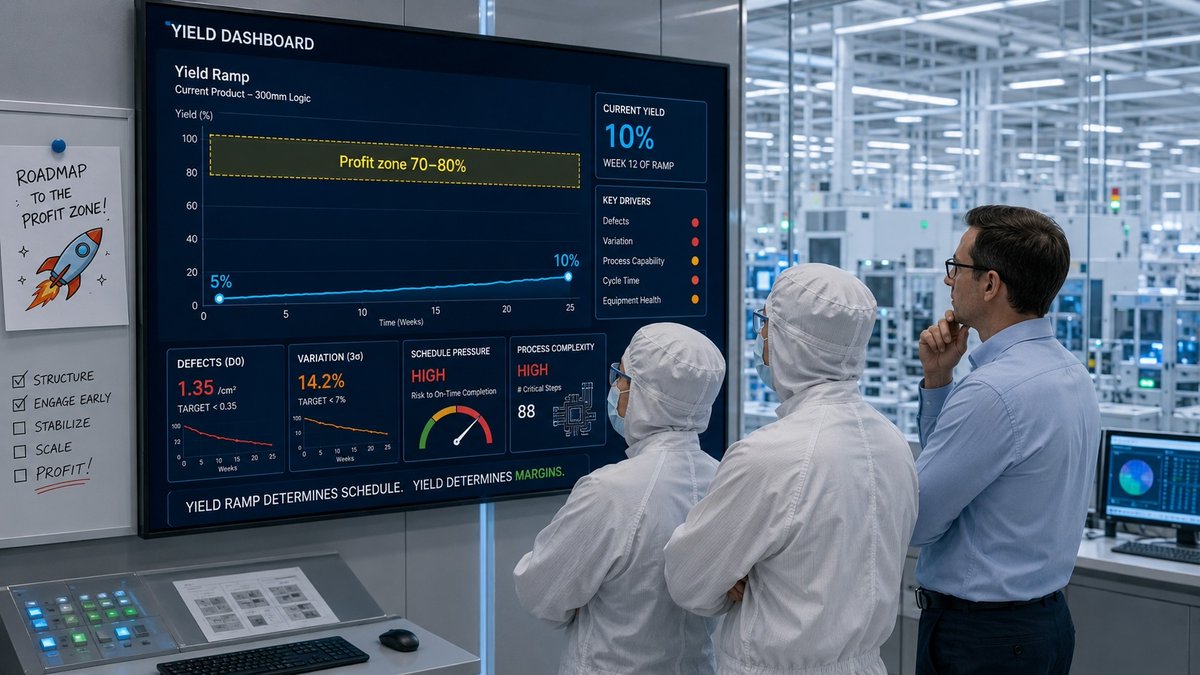
@Intel’s 18A story hides a brutal lesson:
A roadmap can be bold.
A node can be elegant.
A launch can look perfect.
Then yield walks in.
Reuters reported early Panther Lake runs on 18A at ~5% usable chips, improving only to ~10% by mid-2025 – for the node meant to anchor Intel’s manufacturing comeback.
The stack is ambitious: gate-all-around, backside power, advanced packaging, and a new ramp all at once. On slides, that looks heroic. In the fab, every “breakthrough” is a new source of variation.
Yield ramp is where optimism is audited.
Defects do not care about strategy.
Customers care about supply, performance, timing, and confidence.
The deeper question in advanced manufacturing is rarely:
“Can we build it?”
It is:
“Can we build it repeatedly, profitably, and under control?”
That is where the roadmap becomes real.
Problem solving is often treated as an engineering activity.
In complex manufacturing, it behaves more like margin infrastructure.
Every recurring defect hits the P&L through:
scrap, rework, delays, extra inspection, engineering time, customer pressure, capacity loss, and “temporary containment” that becomes permanent process architecture.
Elegant. And expensive.
In semiconductor manufacturing, a small issue can quickly cascade through yield, cycle time, reliability, delivery, and customer confidence before finance sees the full impact.
This is why problem solving deserves a seat at the margin table.
A few “boring” improvements have very real business effects:
• Faster investigation → less production uncertainty
• Stronger root cause reasoning → fewer repeat failures
• Process simplification → less operational drag
• Captured learning → the next team starts above zero
• Robust corrective actions → fewer hidden cost loops
Many companies measure yield, scrap, rework, cycle time, escapes, and cost of poor quality. Far fewer measure the quality of the thinking that shapes those metrics.
Engineering thinking is financial infrastructure.
Margin is protected long before the quarterly report—
when teams understand the mechanism, remove recurrence, and stop turning every problem into more operational complexity.
#EngineeringThinking #Engineering #Manufacturing #Semiconductor #Semiconductors #PRIZGuru
Inside the fab, a yield problem looks like engineering.
On the customer roadmap, it becomes a board-level risk.
@Samsung’s 3 nm gate-all-around process reportedly stayed near 50% yield after about three years of production, while TSMC’s 3 nm was reported above 90%.
That gap does more than change cost per good die.
It changes trust.
Google reportedly moved Tensor G5 to TSMC. Qualcomm and AMD also favored TSMC for advanced nodes. At that level, customers are buying confidence as much as silicon:
* Will we get enough top-bin parts?
* Can we launch on schedule?
* Can we avoid thermal surprises?
* Can we protect our own customer promises?
Yield is often treated as a manufacturing KPI. At advanced nodes, it acts like a competitive weapon.
A weak yield number does not just reduce margin. It quietly trains customers to build their future around someone else’s process.
Then recovery is not only about yield. The fab must restore stability and belief.
That is why yield excursions need more than dashboards and ad-hoc task forces. Teams require structured causal investigation, disciplined process understanding, and learning that survives beyond the emergency.
In foundry, “almost ready” can still be several billion dollars away from “trusted.”
Manufacturing complexity rarely arrives as a villain.
It arrives as something reasonable:
- a new inspection after one escape
- a rework loop after one defect
- a manual approval after one bad change
- a spreadsheet because the system “doesn’t support that yet”
- a workaround an expert “just knows”
Individually, each fix makes sense.
Together, they create a hidden factory inside the real one.
That hidden factory consumes engineering time, operator attention, training, cycle time, and patience.
Many factories treat complexity as maturity: more controls, more gates, more exceptions, more dashboards. Sometimes that is risk management. Sometimes it is operational debt.
A useful question during problem-solving:
“Are we removing the failure mechanism, or adding another layer to survive it?”
Every workaround adds future cost:
• harder training
• more failure modes
• slower troubleshooting
• longer recovery
• weaker ownership
Complexity is dangerous when nobody remembers why it exists, who owns it, or when it can be removed.
The best teams make the system visible before adding another fix:
Map the process.
Map the functions.
Map the interactions.
Then decide if the next action reduces complexity or deposits more debt into the factory.
Complexity does not send a monthly invoice.
It waits—then something breaks.
#Engineering #Manufacturing #Process #ContinuousImprovement #Semiconductor #Semiconductors #RootCauseAnalysis #PRIZGuru
Asking “why?” is useful.
Asking it five times in a complex manufacturing system can still walk you confidently in the wrong direction.
Fabs, assembly lines, chemical processes, and test flows rarely fail as a neat chain:
symptom → cause → root cause → fix
Problems usually live in a network where:
- one parameter drifts
- one control loop compensates
- one inspection hides the signal
- one upstream step shifts the distribution
- one “temporary” workaround becomes standard
- one team sees the defect while another owns the mechanism
This is where linear RCA gets risky. A 5 Whys session can produce a clean answer while missing the system behavior that created the failure.
In complex manufacturing, a better question is:
“What functions, interactions, controls, and tradeoffs allowed this failure to appear?”
Visual and system modeling make scattered knowledge visible. Teams can see components, steps, functions, assumptions, and causal hypotheses as objects they can inspect, challenge, and improve.
Shallow RCA creates shallow corrective actions.
Shallow corrective actions become recurring defects with better documentation.
A complex system needs a system‑level investigation.
Where do you see RCA fail most often: missing the mechanism, oversimplifying the process, or jumping to corrective action too early?
#RootCauseAnalysis #Manufacturing #Semiconductor #QualityEngineering #Process #SystemsThinking #ContinuousImprovement #Engineering #Semiconductors #PRIZGuru
Investors ask semiconductor companies about yield.
That sounds smart.
The better question is: *what kind of* yield?
One headline number can hide very different realities:
- dies that only pass after retest
- dies that need repair
- dies binned down into lower‑margin SKUs
- dies that “pass” but miss the performance that justified the product
For companies like Intel, Samsung Foundry, TSMC, AMD, and NVIDIA, manufacturing quality, bin mix, supply confidence, and margin are tightly linked.
So when you hear “yield is improving,” the follow‑up should sound more like a fab review than a script:
- How much passed first time?
- How much needed retest?
- How much was repaired?
- How much was binned down?
- How much reached top‑bin performance?
- How much failed parametric or final test?
A single yield percentage without this breakdown is just spreadsheet decoration.
The most important yield numbers are usually not in the press release.
They are in the internal mix that shows whether the process is healthy, fragile, or being propped up by retest and heroic engineering.
What yield question would you ask before investing in a chip company?
“We do not have time to model the problem.”
Understandable. When a process drifts, yield drops, or a customer is waiting, the pressure is to act now.
But in complex manufacturing, the time skipped at the beginning usually returns with interest.
A team skips 90 minutes of structured thinking…
Then spends weeks on:
• competing theories
• repeated experiments
• temporary controls
• extra inspections
• meetings that restart the same conversation
• fixes that work just long enough to look convincing
Structured problem solving feels slower because it forces a pause:
What is actually happening?
Where is value being lost?
Which function failed?
Which assumption are we treating as fact?
What must be true for this hypothesis to explain the symptom?
That pause can be uncomfortable, especially for strong engineers who see three fixes before the meeting starts.
But the business rarely needs the fastest first action.
It needs the fastest reliable path to understanding, prevention, and reuse.
In fabs, labs, and complex production, guessing creates motion.
Structured thinking creates direction.
Direction is what stops recurrence.
Structured thinking is slower than guessing.
It is faster than being wrong.
#Semiconductor #RootCauseAnalysis #ProcessEngineering #YieldImprovement #ProblemSolving #Semiconductors #PRIZGuru
Advanced nodes are often described as “smaller.”
Technically true—and incomplete.
The bigger issue is that advanced nodes are less forgiving.
TSMC N2, Intel 18A, Samsung 2nm/GAA all push tighter lithography, new transistor structures, and more complex integration. At these scales, tiny shifts in:
- temperature
- chemistry
- overlay
- etch profile
- deposition uniformity
- contamination
- EUV behavior
can quietly move a chip from:
top‑bin → lower‑bin
passing → marginal
marginal → scrap
ASML keeps advancing EUV, but smaller patterns still amplify randomness, variation, and hidden interactions.
This is why yield at advanced nodes cannot be fixed by “more”: more inspection, more screens, more dashboards, more gates. Controls are necessary, but if the process stays fragile, they become expensive babysitters.
The real goal is a process that is:
- simpler where possible
- stable by design
- understood at the mechanism level
At advanced nodes, the enemy is not only defects.
The enemy is fragility.
A fab can have world‑class dashboards and still have world‑class confusion.
SPC, MES, FDC, yield maps, inspection data, test results — semiconductor teams are not short on signals.
The hard part is turning those signals into a mechanism.
Dashboards can tell you:
• this tool drifted
• this lot behaved differently
• this defect pattern appeared
• this parametric bin shifted
• this chamber looks suspicious
Useful? Yes.
Sufficient? Rarely.
Different teams see different slices: process sees parameters, yield sees maps, equipment sees alarms, quality sees escapes, operations sees delays, management sees margin leaking into scrap and rework.
The data says, “Something changed.”
Reasoning asks, “Which change matters, through what mechanism, under which conditions, and why did the system allow it?”
Dashboards cannot do that thinking for us.
The best teams treat data as evidence and build a structured explanation: functions, process steps, causal links, assumptions, contradictions, decision logic.
Data is the evidence.
Reasoning is the investigation.
Where have you seen teams confuse “we found a correlation” with “we understand the mechanism”?
#Semiconductor #Yield #RootCauseAnalysis #Process #QualityEngineering #Manufacturing #ContinuousImprovement #Semiconductors #PRIZGuru
The most expensive defect is not always the dramatic one.
Often it is the polite defect that returns every quarter in a new form.
In complex manufacturing, especially semiconductors, recurrence is where the real cost hides:
* scrap that “should be temporary”
* rework that becomes routine
* customer delays framed as “one more exception”
* quality escapes that trigger another investigation
* engineers pulled from improvement work to solve the same issue again
A one-time failure says: something went wrong.
A recurring failure says: the system learned too little.
That usually means:
- the symptom was only contained
- the mechanism was misunderstood
- the learning stayed in a meeting, slide deck, or memory
Recurrence is not only a quality problem. It is a signal that the organization’s problem‑solving process has a weak memory.
The answer is rarely “try harder.” It is to make the reasoning visible:
What function failed?
What interaction changed?
Which assumption was tested?
Which cause was eliminated?
Which decision was made, and why?
When the logic is visible, teams can challenge, improve, and reuse it.
Recurrence is the tax companies pay for incomplete understanding.
In manufacturing, that tax compounds.
#Manufacturing #Semiconductor #RootCauseAnalysis #Quality #ProcessImprovement #ContinuousImprovement #Semiconductors #PRIZGuru