TSMC fumbles Copackaged optics for the Nth time like some fucking donkeys and now the whole industry is limping towards NPO, and the pod bros who price the entire AI TAM off Nvidia’s BOM line items still can’t actually explain what the problem is. So let me do the engineering for you, since clearly nobody on here will.
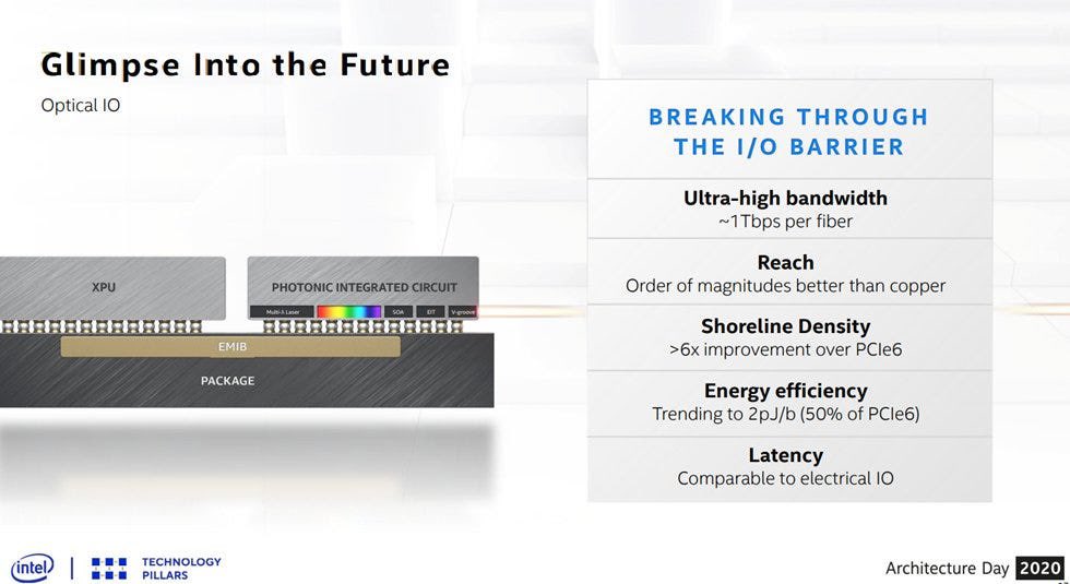
The bottleneck was never can you make light go through a waveguide. It’s all fucking thermals which is downstream of packaging. Specifically, how do you get a photonic engine onto the same substrate as a switch ASIC or XPU without your yield falling off a cliff and your reliability failing.
TSMC’s answer is CoWoS where they bolt everything onto one big monolithic silicon interposer. Cute, until you hit the reticle limit and start duct-taping interposers together (CoWoS-S, then -R, then -L, soon -PleaseStop). Every chiplet and HBM stack you add to that single interposer compounds your defect probability and one bad die leads to a five-figure package going into the dumpster. CoWoS is thermally retarded and the whole industry knows this and it’s why capacity “can’t expand” and Jensen is acting like a bouncer in the front of a club choosing who gets pass the velvet rope.
There is ONLY one company that will make copackaged optics work and expand in the rack… it’s not Lumentum, it’s not Coherent, it’s fucking INTELLLL.
Intel’s EMIB gets rid of a giant reticle limited interposer and replaces it with a tiny silicon bridge that does the high-density coupling locally, exactly where you need it. You localize the hard part and the thermals in one area and your yield is ridiculously high. Comparing EMIB & CoWoS is so funny cause EMIB is north of 95% yield with like 12 reticle size equivalent package while CoWoS falls off a cliff after 5.5 reticles it’s that bad…now imagine adding thermally sensitive photonics.
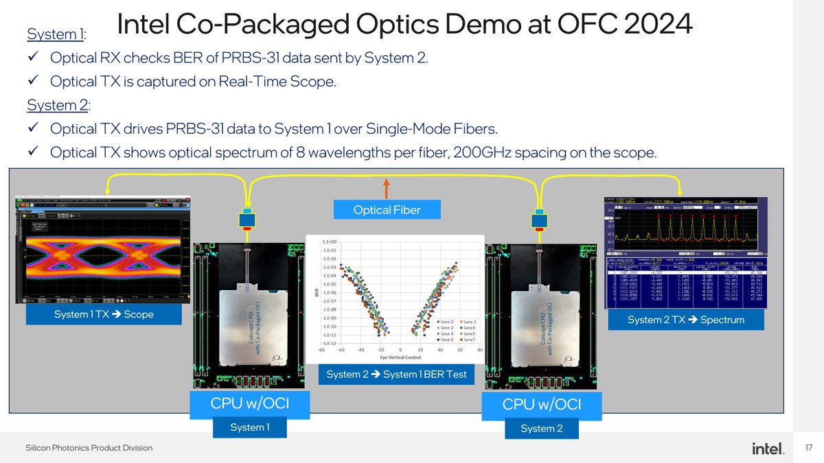
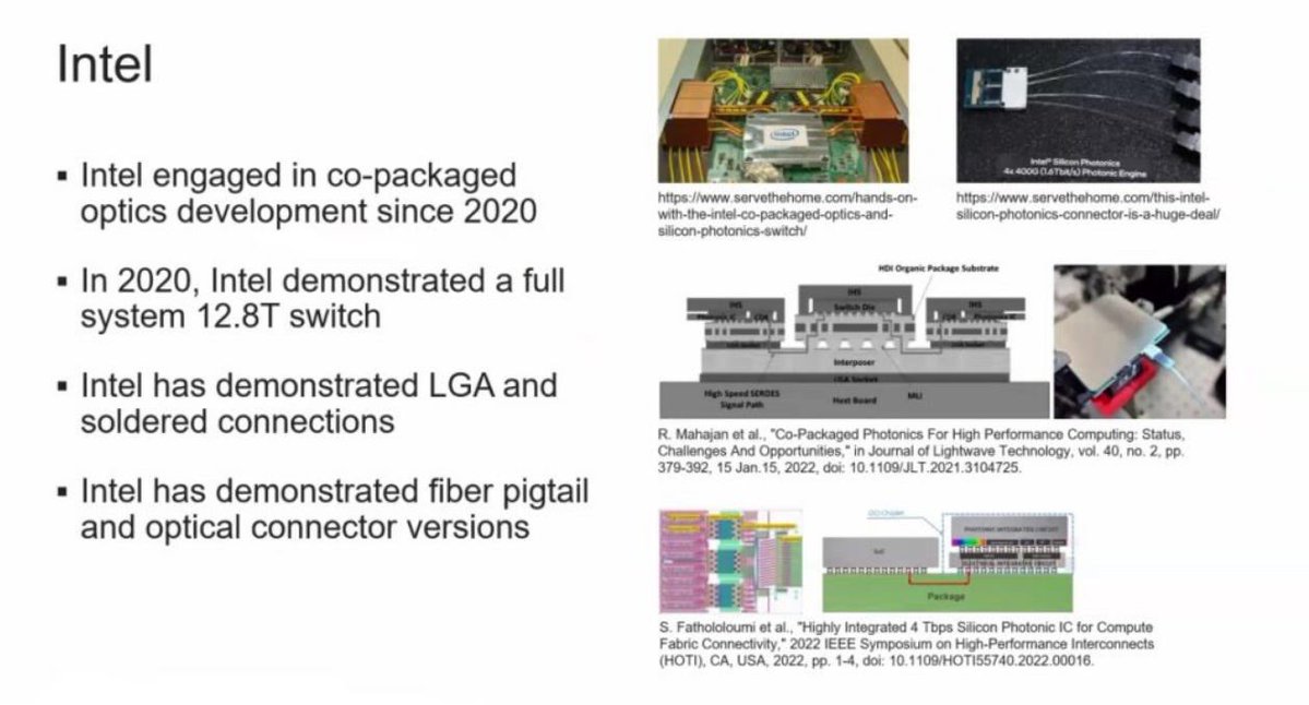
People don’t know this but Intel has been doing silicon photonics in-house for ~25 years... In 2024 they showed an Optical I/O chiplet doing 2 Tbps bidirectionally at ~5 pJ/bit, with the PIC and EIC co-packaged right against the ASIC and it’s all because of EMIB. And even more critically than that, they’ve actually run the fiber-attach and reliability/test flow to JEDEC-grade standards already, which everyone hand-waves until their links flap in production.
My prediction is clear: Intel will capture over 90% of the copackaged silicon photonics market in the next five years because there is NO ALTERNATIVE.
一张图详细了解下FOTO这支应该是美股现在资产管理最小(上市只有3个交易日,50万美金管理规模)的ETF,但也是现在美股里最纯粹的光互连+光子学产业链的高beta主题组合。FOTO优势是主题很聚焦:持仓都和 AI 数据中心光模块、相干光通信、激光器、光学制造、测试测量等环节最核心的产业链公司。而EUV更偏大盘半导体+光学(光互连、光学纯度相比FOTO差不少)。