Circuit Board Design was created to deliver enterprise-grade PCB design discipline with fast, disciplined delivery. Our roots go back to 2016, when we founded E
Designing for a million bend cycles in robotic arms? Solid copper traces in flex zones will fail. Use hatched copper planes and optimized bend radii for million-cycle reliability. DM to connect.
100+ bar subsea pressure destroys standard PCBs. Our underwater sensor nodes use ENEPIG corrosion-resistant traces and custom potting to survive the deep ocean.
Designing for 480V grid interfaces under IEC 61850? If your creepage and clearance distances ignore isolation slots, arcing will fail your prototype. Don't skip the physical milling.
Need decades of unattended power for remote aerospace nodes? We integrate diamond betavoltaics directly onto custom multi-layer PCBs. DM us for your layout.
BGA solder wicking destroying yields? IPC-4761 Type VII plugged & capped via-in-pad (VIPPO) delivers flat, planar pads. Eliminate voids and secure your dense multi-layer assemblies.
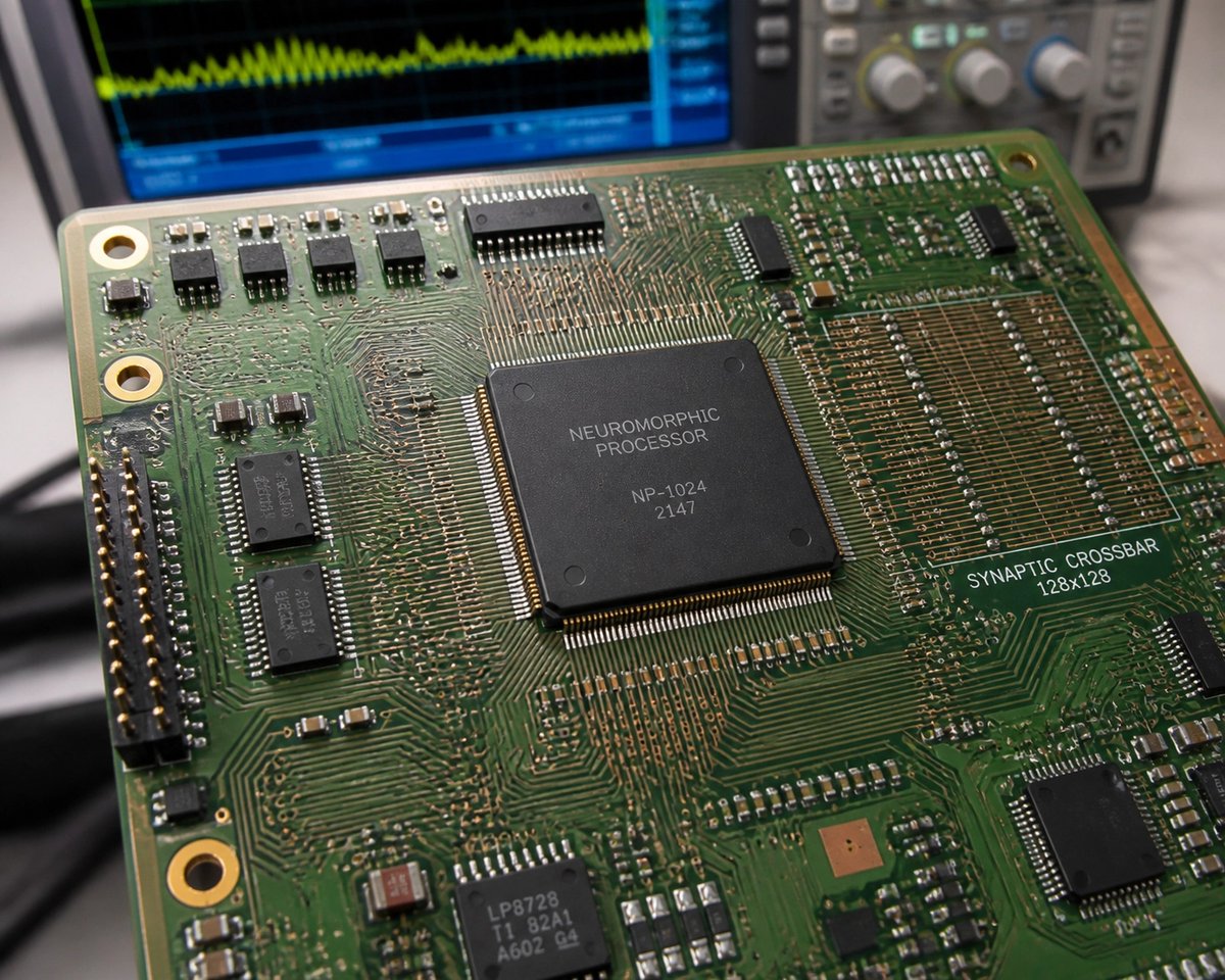
Routing dense synaptic crossbar arrays for SNNs? Managing multi-layer interconnects without signal degradation demands strict impedance control. How do you handle your high-density routing? DM us ⚡
Designing an EV BMS? Skip standard traces for cell voltage balancing. Use 3-wire Kelvin sensing and heavy copper busbars to eliminate voltage drop errors in high-current automotive power stacks.
Designing 20-yr reliable PZT sensor interfaces for bridge SHM requires robust lightning surge protection & IP68 sealing. We engineer hardware built to outlast the elements.
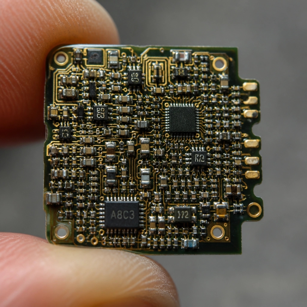
Fitting a complete audio DSP and wireless stack onto a 10mm² flex PCB is brutal. We achieve it with ultra-dense multi-layer routing and biocompatible ENIG finishes for medical reliability.
Integrating solid-state LiPON cells on your PCB? Precise cavity routing and high-current busbars prevent trace dissolution under thermal loads. How do you handle your energy storage layouts?
Managing flux noise at 4K? Niobium shielding via the Meissner effect is critical for superconducting qubit layouts. Complete magnetic field expulsion protects your sensitive quantum hardware.
Moving from a dev kit to an 8-layer HDI board? Don't let layout bottlenecks stall your prototype. Robust EDA infrastructure and strict DFM validation before file release save weeks of respins. Let's talk layout.
AI automates 80% of routine DRC checks on 16-layer boards. But high-speed routing, return paths, and EMI compliance still demand expert human engineering judgment. Don't trust AI blindly.
24-hour bare boards or 5-day HDI builds? Speed tradeoffs cost millions if DFM fails. We validate Altium layouts against real fab rules before release to kill prototype surprises.
CH32V006 layout pitfall: Watch for VCC/VDD pin swaps & missing EN pull-ups causing 3.3V rail collapse on Rev A. Get your first spin right with IPC CID+ design expertise.