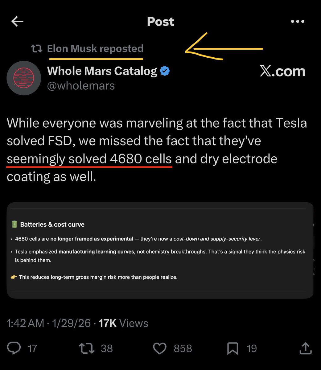
BREAKING 🚨 TESLA LOCKS DOWN THE "SECRET RECIPE" FOR ITS DRY ELECTRODE MANUFACTURING 🔒
For years, the battery industry believed that mass-producing dry electrodes was impossible, a lab trick that simply couldn't scale.
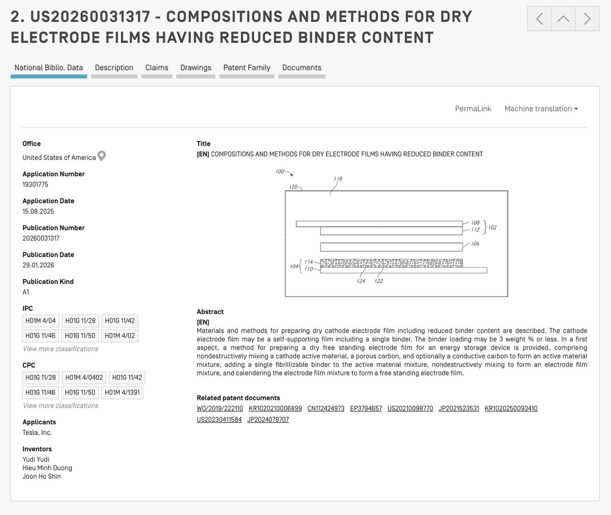
Published on January 29, 2026, patent application US20260031317A1 proves them wrong and reveals the next, ruthless phase in Tesla's intellectual property strategy.
If the previous patent was about owning the car, this one is about owning the factory. This filing serves as the definitive "cookbook" for the holy grail of battery manufacturing.
While Tesla has already secured the rights to the superior performance of the battery, this continuation protects the method. By patenting the exact order of operations and physical constraints required to ditch toxic solvents, Tesla is effectively copyrighting the "kitchen" so that no one else can bake the same cake.
This ensures that even if competitors figure out what makes the dry electrode work, they will be legally barred from using the most efficient way to make it.
To understand why this legal firewall is so necessary, we have to look at the specific engineering trap that Tesla is trying to prevent competitors from exploiting.
🧩 The problem: Copying the result, evading the method
The transition from "wet" to "dry" manufacturing is notoriously difficult because of a cruel physical trade-off: to make dry powder stick together into a solid sheet, you typically need to apply high-shear force or add large amounts of polymer "glue".
Both are bad. High shear crushes the delicate battery crystals (killing lifespan), while excess glue wastes space (killing range).
Tesla has solved this by developing a "Goldilocks" zone, a gentle mixing process that activates the binder without destroying the particles. However, this creates a legal vulnerability.
In the world of patents, securing the "end product" (a high-efficiency battery) is a massive win, but it leaves a loophole. Competitors could theoretically try to achieve similar battery performance using a slightly different, less efficient, or messier process to skirt the patent rules.
If Tesla only protects the final battery, rival manufacturers could reverse-engineer the specifications while claiming their production line is "different enough" to avoid infringement.
To truly secure its competitive advantage, Tesla needs to protect the unique, low-cost "kitchen" where the battery is made, not just the "cake" that comes out of the oven. To close this specific loophole, the new filing moves to secure the manufacturing process itself.
💡 Tesla’s solution: The "method" is the moat
Tesla’s solution, detailed in this continuation, shifts the legal focus from the device to the method of fabrication. This effectively means Tesla is moving from protecting the final battery product to patenting the specific recipe and cooking steps used to make it.
The key innovation here is not just that the electrode works well, but that it is manufactured using a specific, counter-intuitive sequence. The patent application seeks to protect a method that involves nondestructively mixing active materials with porous carbon first.
These active materials are the primary lithium compounds that actually store the energy, while the porous carbon acts as a conductive additive that functions like a microscopic electrical grid.
The process uses nondestructive mixing, which is a gentle blending technique that mixes the ingredients without crushing them, much like folding ingredients into a cake batter to keep it airy.
Only after this initial blend is complete does the method involve adding the dry binder to create the final film. This dry binder is a polymer adhesive that serves as the structural glue to hold the powder mixture together in a solid sheet.
By legally defining this specific order of operations, specifically mixing the dry energy-storing ingredients before introducing the glue, Tesla is fencing off the most logical and efficient way to produce dry electrodes. This prevents competitors from adopting Tesla’s streamlined manufacturing flow, forcing them into less efficient, more complex, or more expensive production methods.
But the "method" is only half the story; the other half relies on the specific physical characteristics of the ingredients themselves.
🔬 The innovation: Large particles and "gentle" manufacturing
This filing doubles down on a specific physical constraint regarding the size of the particles used in the battery. The patent explicitly claims protection for using active material particles that are at least 10 microns in size. For context, ten microns is roughly one-tenth the width of a human hair.
This is significant because traditional battery manufacturing often relies on pulverizing materials into fine dust to make them fit into a wet slurry, which is essentially a muddy paste created by mixing powders with liquid solvents.
Tesla has discovered that by keeping the particles larger and pristine, they can use significantly less binder. Specifically, they use less than 2% by weight of this binding glue.
The patent describes a process where these larger particles serve as the structural bricks of the electrode wall, while the PTFE binder acts as the minimal mortar. PTFE (polytetrafluoroethylene) is the same polymer found in non-stick cookware.
To achieve this structure without cracking the large particles, the method specifies using acoustic or low-speed blade mixers running at a crawl of 10 to 40 meters per minute.
Acoustic mixers use sound energy to vibrate and blend materials without direct contact, while blade mixers gently fold the powder like a slow-moving dough hook. This nondestructive approach is now a core part of the claim, ensuring that the method itself is recognized as a unique invention because it preserves the original quality of the materials.
With the physical method established, Tesla tightens the noose further by adding strict chemical rules that make the patent nearly impossible to sidestep.
📝 The fine print: Three critical constraints
To truly lock out competitors, this continuation filing adds three hyper-specific "fences" around the manufacturing process that move beyond general concepts to define the exact chemical and physical limits of Tesla's technology.
First, the patent imposes a strict "Single Binder" rule. While many battery manufacturers use a cocktail or complex mixture of glues to balance adhesion and flexibility, often mixing PTFE with other polymers like PVDF (polyvinylidene fluoride) or CMC (carboxymethyl cellulose), Tesla’s filing explicitly prohibits this.
The text specifies that the binder "consists essentially of a single dry fibrillizable binder". A fibrillizable binder is a material capable of forming a microscopic web of fibers when mechanically stressed.
This forces the recipe to rely 100% on the mechanical fibrillation of PTFE, a process that physically stretches the binder particles into thread-like networks rather than relying on chemical stickiness. It asserts that their process is so refined they don't need the chemical crutch of secondary glues.
Second, Tesla places a hard legal ceiling on conductive carbon. This carbon serves as an electrical pathway but acts as a "dead weight" filler because it does not store any power itself.
The patent caps this material at "at most 8 wt%", meaning it can comprise no more than eight percent of the total weight of the electrode. While carbon is essential for electricity to flow, it stores no energy.
Competitors might try to make a dry electrode work by dumping in 15-20% carbon to compensate for poor connectivity, but that results in a mediocre battery with less room for active ingredients. By setting this limit, Tesla protects the high-performance version where filler is kept to a bare minimum to maximize energy density, which is the amount of energy stored relative to the battery's size.
Finally, the filing reveals a "Hero" configuration that proves this process isn't just for lower-end standard batteries. It details a specific formula using 98% NMC 811.
NMC 811 refers to a lithium nickel manganese cobalt oxide chemistry rich in nickel, which is difficult to handle but offers superior range. This formula combines that high-performance material with just 1.25% PTFE binder and 0.75% total carbon.
Achieving a stable film with such a high load of active material proves this dry process is ready for Tesla's most demanding vehicles, effectively turning the electrode into a nearly solid block of energy.
Once this highly specific mixture is prepared, the final step of the process seals the advantage by defining the speed of production.
⚡ The "3-pass" efficiency
A critical detail in this continuation is the speed of formation. The filing highlights that this specific recipe allows the dry powder to be turned into a self-supporting sheet, meaning the film is structurally sound enough to be handled like a roll of fabric without crumbling or needing a supporting metal foil.
This result is achieved after passing through a process called calendering, which involves feeding the material through a series of heavy steel rollers that press it flat, much like a pasta machine flattening dough. The patent specifies this happens at most three times.
In manufacturing, fewer passes equals higher speed. By claiming a process that creates a sturdy film in just three steps, Tesla is effectively patenting the velocity of its production line. This velocity determines the overall factory throughput, or the volume of finished product made per hour.
A competitor trying to replicate this might need 10 or 20 passes to get a stable film. This requirement would force them to run the material back and forth repeatedly, making their factories slower and more expensive to run than Tesla's.
This combination of legal, chemical, and manufacturing speed constraints lays the foundation for Tesla’s dominance in the next decade.
🚀 How this continuation contributes to Tesla’s now and future
First, it blocks competitors from "fast-following" the 4680 production method. While other automakers can buy good batteries, this patent prevents them from building factories that operate like Tesla’s. By protecting the specific "mix-then-bind" sequence and the "low-binder" recipe, Tesla ensures that its Gigafactories remain unique. Competitors cannot simply buy the same mixing equipment and run the same recipe without risking patent infringement.
Second, it secures the economics of "cheap" raw materials. By specifically patenting the use of larger (greater than 10 microns) particles, Tesla is validating a cheaper supply chain. Smaller, highly processed particles cost more. This patent confirms that Tesla’s process is optimized for standard, "bulk" grade materials. Protecting this capability ensures Tesla retains a cost margin advantage, as they can turn cheaper, commoditized inputs into premium performance outputs.
Third, it creates a legal "thicket" around dry electrode tech. This filing is a classic "picket fence" strategy. The parent patent protects the battery efficiency (90-94%). This child patent protects the binder loading (less than 2%) and the particle size. Future filings will likely protect the machinery. This layering makes it nearly impossible for a competitor to design a dry electrode without tripping over at least one of Tesla’s patents.
Finally, it validates the "micro-factory" concept. The emphasis on creating a "free-standing" film without a metal foil backing is crucial. It means the electrode film can be made in one machine and rolled up, then applied to foil later. This decouples the manufacturing steps, allowing Tesla to fit production lines into smaller, non-linear spaces, which is essential for the tight footprints of future factory expansions or retrofitting existing lines.
READ IT TO BELIEVE IT 🚨 TESLA HAS ENGINEERED A "THERMAL ARMOR" THAT ALLOWS SILICON CARBIDE CHIPS TO SURVIVE 800V SURGES ⚡️
Under the hood of Tesla’s next-gen powertrain lies a heavy copper secret.
While most chip innovations focus on the microscopic silicon inside, Tesla’s latest breakthrough completely reimagines the protective shell around it.
Originally revealed in late 2024 (Patent WO 2024/197013) and confirmed by a new European filing published just days ago on January 28, 2026 (EP4684423), this novel "hybrid" package architecture turns the chip's casing into an active thermal battery.
The invention is known as a "Semiconductor Package with Top-Side Heat Spreader". It uses a massive, stepped-copper block that occupies nearly the entire top surface of the device.
This architecture allows the chip (Silicon Carbide chip) to absorb the instantaneous heat of a 0-60 launch or a Supercharging session. By doing so, it protects the delicate electronics inside without the need for exotic cooling systems.
Before diving deeper, it is critical to distinguish this technology from the "advanced packaging" often associated with Tesla's AI hardware. While chips like the AI5 computer are the vehicle's "brain", the technology in this patent represents the vehicle's "muscle".
The AI chips are delicate supercomputers packaged by TSMC to move massive amounts of data. In contrast, the chips in this patent are rugged power switches responsible for moving energy to the motors and accessories. They require a completely different architectural approach. This approach focuses on raw survival rather than just speed.
To understand why this radical redesign is necessary, we first need to look at the invisible physical wall that these standard automotive chips have hit.
⚖️ The problem: Standard chips can't handle 2026-era power density
In 2026, the Power Dual Flat No-lead (PDFN) package remains the unglamorous workhorse of the automotive industry. This is due to its low cost and compact footprint. However, as electric vehicles aggressively move toward 800V architectures and silicon carbide chips, this standard design has hit a physical limit.
These packages lack the internal thermal mass to absorb the massive "surge loads" generated when a motor accelerates or a heat pump kicks in. This causes chips to hit their thermal limits milliseconds before the vehicle's cooling system can even react.
Compounding this thermal bottleneck is the legacy "gull wing" lead design still common in automotive chips. These conductors bend up and out like a bird's wings. This shape introduces unnecessary length to the electrical path.
In the era of high-speed switching, this extra length creates parasitic inductance. This is a form of electrical friction that generates noise and wastes battery range. While suitable for older and slower electronics, this geometry acts as a drag on the efficiency of modern wide-bandgap semiconductors that need to switch thousands of times per second.
Finally, the manufacturing process for these power chips has failed to keep pace with the efficiency demanded by the rest of the vehicle production line. The industry currently relies on a "messy" traditional method. This involves encapsulating chips in plastic blocks and then grinding them down to expose the metal. This process is inherently wasteful and slow.
Tesla faced a gap in the market. They needed a solution as rugged and cheap as a standard PDFN, but with the thermal resilience of a heavy-duty power module.
Here is how they engineered that exact contradiction.
💡 Tesla's solution: A hybrid design with a massive thermal roof and a flat electrical floor
Tesla’s engineers have developed a semiconductor package that fundamentally changes the ratio of materials used. This package is the protective casing that connects the delicate silicon chip to the rest of the vehicle's electronics.
Instead of keeping the materials at a uniform thickness throughout the device, the design places a massive "die paddle" or heat spreader on the top of the chip. This paddle functions like a heavy copper roof that draws heat away from the sensitive electronics.
This structure creates a device that is optimized for two different functions simultaneously. The top section is a heavy thermal sink designed to absorb heat shocks. You can think of this as a thermal sponge that soaks up sudden bursts of temperature before they can damage the chip.
On the bottom, the design utilizes very thin and flat leads to create a streamlined electrical path designed for speed and efficiency. Crucially, the design is "molded to net shape". This manufacturing term means the part comes out of the mold in its final ready-to-use form. This effectively eliminates the need for expensive post-processing steps like grinding or sawing.
The most visible part of this new architecture is the sheer volume of copper on top. This serves a critical protective purpose.
🧱 The heat spreader acts as a thermal battery for surge loads
The defining feature of this patent is the thickness of the top-side heat spreader. This component is a solid block of metal designed to pull heat away from the chip's hot core.
Tesla specifies that this copper block must be at least 1.5 times thicker than the electrical leads. These leads are the thin metal pins that carry current in and out of the device. In some embodiments, the block is up to 3 times thicker than these connections.
Crucially, this is not a small insert. The patent mandates that the exposed heat spreader occupies at least two-thirds and potentially up to 80% of the package's entire top surface.
When a power surge occurs, this thick block of copper acts like a buffer. A power surge is a sudden and intense spike in electricity that generates immediate heat. The copper absorbs this spike in thermal energy instantly. It does this in the same way a thick stone wall absorbs the heat of the sun without getting hot on the inside.
This prevents the temperature of the delicate silicon chip from skyrocketing. This architecture enables true "Top-Side Cooling". This is a method where heat is pulled off the top of the chip rather than the bottom. It allows Tesla to dissipate heat directly into a heatsink. A heatsink is a metal radiator that disperses the heat into the air or cooling fluid. This is much more efficient than forcing the heat down through the crowded circuit board.
But sheer mass isn't enough. The internal geometry of that copper needs to be precisely sculpted to ensure the device survives years of operation.
🧩 Internal architecture: Grooves, forks, and cutaways
Tesla’s engineers didn’t just place a block of copper on top. They sculpted the internal surfaces to manage the flow of liquid metal during assembly. The patent details a specific "groove" etched into the inner surface of the heat spreader.
This groove acts as a "solder stop". It functions like a microscopic dam that prevents the molten attachment material or metal glue from bleeding out into unwanted areas.
Additionally, the die paddle features a specific cutaway region or stepped profile. This shape resembles a staircase. It allows the copper to overhang the chip edges for maximum volume while still locking securely into the molding compound. The molding compound is the hard plastic shell that encases the electronic components.
Furthermore, the patent introduces a "forked" lead frame design. In this configuration, the copper connections do not just sit next to the chip. They "straddle" or fork around the sides of the silicon die. The silicon die is the tiny square of silicon that performs the actual switching.
This geometry allows Tesla to wrap the die in "thermal mass". This refers to the material's ability to absorb and store heat energy from the sides as well as the top. This creates a "conductive brim" that acts like a heat-absorbing rim around the chip. It squeezes every bit of capacity out of the small package footprint.
While the top of the package manages the thermal load, the bottom attacks a completely different foe: electrical inefficiency.
⚡ Flat leads significantly reduce parasitic inductance
To solve the electrical efficiency problem, Tesla has ditched the "gull wing" design entirely. This is a traditional shape where the metal connectors bend up and out like the wings of a seagull.
Instead, they utilize a lead frame with flat and stamped leads that sit flush with the bottom of the package. The lead frame is the metal skeleton that supports the chip and carries the current. By removing the bends and loops found in traditional connectors, they have shortened the physical distance the current must travel.
This reduction in path length directly lowers the parasitic inductance. This is a form of unwanted magnetic energy or "electrical inertia" that builds up when electricity travels through long loops. It resists rapid changes in current.
In power electronics, lower inductance reduces the loop area. This allows the switch to turn on and off faster with less energy loss. The patent explicitly notes that this architecture is desirable for "wide-bandgap semiconductors". These are advanced materials that can operate at higher voltages and frequencies than standard silicon. Specifically, the patent mentions "bidirectional GaN HEMTs" or Gallium Nitride High Electron Mobility Transistors. This hints that Tesla is optimizing these packages for the next generation of high-speed and high-efficiency switches.
Achieving these complex internal shapes usually requires expensive and slow manufacturing techniques. However, Tesla found a shortcut.
🏭 Stamping technology replaces complex etching and grinding
The patent reveals a focus on high-volume manufacturability. This is the ability to mass-produce millions of units quickly and reliably. Rather than using chemical etching or grinding, Tesla is using stamped metal frames. Chemical etching is a slow process that uses acid to dissolve metal into specific shapes. Grinding is a wasteful technique that mechanically sands away excess plastic to expose the metal.
The top heat spreader and the bottom leads are stamped from metal sheets using a machine that works like an industrial cookie cutter. This creates a "stepped" profile. This is a three-dimensional shape with different height levels similar to a staircase.
These pre-formed shapes allow the components to lock together during the molding process. The design includes "mold locks" and grooves. These act as mechanical anchors to prevent the plastic and metal from delaminating, or peeling apart like layers of old plywood.
Because the parts are stamped to the exact right height, the package creates a tight seal against the mold tool. The mold tool is the hollow metal cavity where the liquid plastic is injected. This results in a finished part that needs minimal cleanup and generates very little waste.
Once these stamped parts are made, they still need to be put together without microscopic errors.
🧘 Smart assembly: Tolerance-absorbing construction
One of the hardest parts of chip packaging is dealing with tolerance. This refers to the permissible limit of variation in the physical dimensions of a manufactured part. Specifically, it refers to the microscopic height differences in the components.
Tesla’s solution utilizes a "stepped height" design where the components are stacked with a compliant paste or solder. This is a soft and pliable bonding material that acts like a mechanical suspension system to cushion the parts.
The patent describes a process where the assembly stack is designed to "float" slightly. This allows the layers to shift and settle naturally before being permanently locked in place. When clamped in the fixture, the compliant bonding material compresses elastically. The fixture is the rigid metal tool used to hold the assembly steady. This means the material squishes down like a spring to absorb the tiny height variances of the die and the copper frames.
This action allows the stack to "self gap-fill". This is a mechanism where the material automatically expands or contracts to bridge any empty spaces between the layers. This ensures that every single package comes out of the machine with the exact same total height. This precision eliminates "flash". Flash is the thin layer of excess plastic leakage that often seeps out of the mold defects and plagues traditional molding processes.
But precision manufacturing is useless if you cannot verify it quickly on the production line.
🔍 Dimples and flanks allow for easy inspection
A subtle but important detail in the design is the inclusion of "wettable flanks" and stamped "dimples" on the flat leads.
A dimple is a small indentation pressed into the metal that provides a dedicated cavity for solder to flow into. Solder is the conductive metal alloy that melts to glue the electronic components together. The wettable flank is an exposed metal side that allows the solder to "wick" up the side of the chip. This means the liquid metal flows upwards against gravity. It is similar to how oil travels up a lamp wick to create a visible fillet on the side of the connection.
This feature is vital for automotive reliability. It allows "automated optical inspection systems" to easily verify that a chip is soldered correctly. These systems are high-speed robotic cameras that scan the manufacturing line for defects.
It also strengthens the physical bond between the heavy copper package and the circuit board. This ensures the chip does not shake loose due to the constant mechanical vibrations of the road.
So, what does this specific piece of copper and silicon actually allow Tesla to do in the real world?
🚀 How this patent contributes to Tesla's now and future
This patent serves as a "unifying architecture" for Tesla’s entire power electronics strategy. It effectively reinvents the standard PDFN package to solve the thermal and electrical bottlenecks that constrain 2026-era vehicles.
By retaining the compact footprint and low cost of the commodity PDFN but gutting its internal structure, Tesla allows the company to solve two different problems. They solve ruggedness for high-voltage traction and efficiency for low-voltage control using a single and scalable packaging platform.
First, it directly addresses the "thermal surge" limit that plagues standard PDFN chips in 800V traction inverters. By replacing the thin and heat-choking lead frame of the legacy design with the massive copper heat spreader described in the solution, Tesla creates a thermal buffer. This buffer absorbs millisecond-long heat spikes before they can damage the die.
This allows Tesla to utilize these compact and cost-effective packages for the heavy-duty powertrains of the Cybertruck and Semi. It allows them to push these vehicles harder during acceleration without hitting the thermal safety limits that would normally require expensive and bulky power modules.
Simultaneously, the patent’s "flat lead" geometry eliminates the "gull wing" inefficiencies of the traditional PDFN. This solves the parasitic inductance issue for the 48V architecture used in steering and auxiliary systems.
These systems rely on Gallium Nitride (GaN) chips that switch at blinding speeds. The removal of the old gull-wing loops provides the clean electrical path these chips need to operate without interference. This enables Tesla to strip copper weight out of the wiring harness while still using a mass-producible package. It proves that they don't need exotic new formats to innovate. They just needed to perfect the one everyone else was already using.
📣 $PIXFI Deposits via ETH Network are open with @pixelverse_xyz
Listing time: Jul 18, 12PM UTC. Stand a chance to grab a share of the 400,000 $USDT Prize Pool
🎁 Token Splash: https://t.co/pcjvVVNlGd
🌐 Learn More: https://t.co/jcdmixdjV5
#TheCryptoArk#BybitListing
Pixelverse will be listed on Bybit, register to create your Bybit account using this official link: https://t.co/sPMehJekAi and grab your share of the 400,000 $USDT prize pool
#pixelverse $PIXFI