@dasnake Also, cvc is only free to use for none commercial projects, which makes it great for say Tiny Tapeout projects but prohibits in for potentially commercial tapeouts.
So as you said, we do still have a partial on SDF sims.
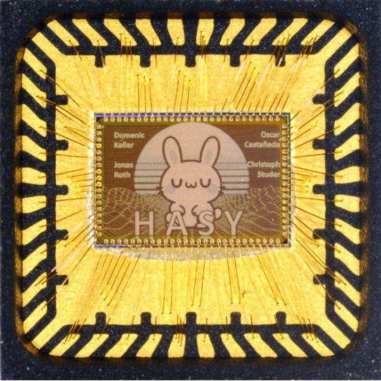
Your daily dose of ASICs.
Open source FPGA, after an open source software stack, the next frontier is silicon.
This board was made by Leo Moser (not me), and manufactured through https://t.co/xkn8rh38JX on the Global Foundries 180nm node.
And it works.
1/2
@dasnake Personally I use icarus verilog for my post-implem gate level simulations. But I am very digital focused, people doing more analog have there own spice flows on top.
(2/2)
Internally this FPGA features:
- 48x I/Os
- 480x LUT4 + FF
- 60x MUX
- 6x SRAM 512x8
- 6x MAC, 8bit*8bit + 20bit
- 12x Register file, 32x4bit each
- 1x Global clock network
All the design files for this chip can be found here:
https://t.co/oOucyZFBL6
Your daily dose of ASICs:
The team from ETH-Zurich's Integrated Information Processing lab (IIP-ETHZ) strikes again!
Bringing us more top tier chip art (and a great paper on designing better audio synthesizers).
Research: https://t.co/ZZWqyyFJu1
Credit for this beautiful work goes to:
- Amanda Krieger (lead author)
- Kennedy Caisley
- Maurice Garcia-Sciveres
- Carl Grace
- Timon Heim
- Zhicai Zhang
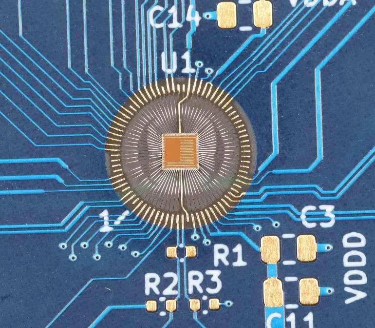
Your daily dose of ASICs:
Behold BigRock and it's stunning circular Chip-on-Board packaging.
This is an analog front end test chip designed on a 28nm CMOS process.
Original paper: https://t.co/p71kAL92nx
@Peter_Hoagins Like often, the node name is marketing.
The boards with this die are still prototypes. I would recommend following Leo on LinkedIn for staying the most up to date with the project: https://t.co/qHmD5BiI9e
I will likely also relay major updates.
Your daily dose of ASICs.
Open source silicon is becoming a reality:
here is a raw die of Leo Moser's open source FABulous FPGA.
github: https://t.co/oOucyZFBL6
@Peter_Hoagins Maybe future versions might be a bit denser but this is a 500nm node at the end of the day.
The easiest scaling would come from moving to smaller nodes.
@idanbeck Tiny Tapeout is a shuttle where multiple projects share the same die making it possible to tapeout at an accessible cost.
This project is for a full independent chip, and the die is as big as a Tiny Tapeout shuttle chip.
It was fabbed on gf180 though https://t.co/xkn8rh38JX.