CW lasers with strong growth through 2030.
"During 2025-30F, demand for CW lasers of 100mW and above is expected to record strong growth, in our view. By 2030E, the market size of CW lasers of 100mW and above is projected to reach USD6.6bn, representing 65.3% of the total market, according to CIC."
Nomura: Optical
Market Overview & Growth Projections
> Revenue Expansion: The global datacenter optical transceiver market is projected to reach USD 47.7bn in 2026F and surge to USD 144.2bn by 2028F, representing a rapid CAGR of 74% from 2026 to 2028F.
> Primary Growth Catalyst: Market expansion is primarily driven by robust, buoyant demand coming from large language model (LLM) training and inference workloads.
High-End Transceiver Shipment Forecasts
High-end speeds (800G and 1.6T) are experiencing stronger momentum due to accelerated technology upgrades within AI networking segments:
> 800G Transceivers: Projected shipments stand at 33.8mn units in 2026F, scaling to 55.0mn units in 2027F, and 78.0mn units in 2028F.
> 1.6T Transceivers: Projected shipments stand at 26.1mn units in 2026F, increasing to 71.5mn units in 2027F, and reaching 126.0mn units by 2028F.
> Next-Generation Speeds (2.4T / 3.2T): Initial shipments are expected to commence in 2027F and 2028F, ultimately reaching volumes of 5mn units and 2mn units respectively by 2028F.
Architectural Evolution & Supply Chain Dynamics
> Co-Packaged Roadmap: As the industry migrates toward co-packaged optics, deliveries of NPO (Near-Package Optics) and CPO (Co-Packaged Optics) products are expected to start rolling out between 2027F and 2028F, serving as fresh demand multipliers for high-power optical lasers.
> Supply Chain Constraints: Unprecedented demand cycles continue to pressure optical chip suppliers' fulfillment capabilities, giving IDM players like Yuanjie a competitive edge in a supply-constrained market environment.
$COHR $LITE $AAOI $MTSI $AVGO
Nomura: NVIDIA Quantum 3400 X800 CPO Switch Component Breakdown
> Total Value: The overall value for the switch components is $83,200 (100% value share).
> Highest Value Component: The 1.6T Optical engine accounts for the largest share at 43% ($36,000 total value, with a quantity of 72 and an ASP of $500).
> ELS Module: Represents the second-highest value share at 22% ($18,000 total value, with a quantity of 18 and an ASP of $1,000).
> 28.8T Switch Chip: Holds a 14% value share ($12,000 total value, with 4 units at an ASP of $3,000).
> FAU and MPO & Fiber: Both components share identical metrics, each accounting for 9% of the value share ($7,200 total value each, with 144 units at an ASP of $50).
> CW Laser: Contributes $2,160 in total value (quantity of 36 at an ASP of $60).
> Shuffle Box: Accounts for the smallest major component share at 3% ($2,800 total value, with 4 units at an ASP of $700).
$NVDA $LITE $COHR $TSM
J.P. Morgan: TSMC CoWoS
CoWoS Capacity Expansion
> Capacity Increase: J.P. Morgan is raising its CoWoS capacity estimates for 2026–2028 by 1%, 9%, and 11% respectively.
> Targets: TSMC’s CoWoS capacity is expected to reach 115k, 190k, and 225k wafers per month (wfpm) by the end of 2026, 2027, and 2028.
> Strategic Shifts: TSMC is accelerating expansion at AP7 Phase 2 (reallocating capacity from SoIC to CoWoS) and is selectively outsourcing interposer manufacturing to Vanguard.
> OSAT Role: Capacity for CoWoS-like processes at Outsourced Semiconductor Assembly and Test (OSAT) providers is expected to reach 15k, 50k, and 85k wfpm by the end of 2026, 2027, and 2028, primarily to support server CPU packaging.
3D SoIC and CoPoS Outlook
> 3D SoIC: The capacity ramp is now more focused on 2028 (projected 65k wfpm) to align with mass adoption in accelerators. While 2027 may see a slight push-out to accommodate CoWoS demand, key customers like AWS, OpenAI, Meta, and NVIDIA (Feynman versions) are expected to adopt SoIC in 2028.
> CoPoS: This technology is currently in the engineering stage. Risk production is expected in early 2028, with mass production likely in 2029.
Customer Demand and Forecasts
> NVIDIA: CoWoS allocations for NVIDIA are rising, reflecting strong demand for new CPUs (Vera in 2027, Rosa in 2028) and accelerators. All NVIDIA accelerator and Co-Packaged Optics (CPO) products are on CoWoS-L at TSMC.
> AMD: Estimates for AMD are rising significantly in 2027–2028, driven by the Venice server CPU family, which will largely utilize a CoWoS-L-like process from ASE.
> CPUs and ASICs: Server CPUs (e.g., NVDA Vera, AMD Venice) have emerged as a primary upside catalyst for CoWoS demand in 2027. Other programs like Google’s TPU and AWS’s Trainium continue to ramp, though ASICs for companies like Microsoft and Meta remain at a smaller scale.
> Supply Chain Roles: AWS and Alchip are expected to remain the primary suppliers for the Neuronlink and UALink versions of Trainium 4. Marvell may take on some share for specific variants that utilize "NVLink fusion" based interconnects. While Trainium 4 volumes in 2028 are expected to be relatively flat compared to Trainium 3 volumes in 2027, the wafer consumption and average selling prices (ASPs) for these chips are expected to be significantly higher.
> 2027 as a Key Ramp Year: While TPU and Trainium are currently the only large-scale ASIC programs, 2027 is viewed as a key year for others to ramp, with a heavy focus on Meta’s MTIA and Microsoft’s Maia.
Other Technological Notes
> Intel EMIB: Intel’s EMIB-T process is seeing incremental demand, notably for the MediaTek TPUv9 Humufish. However, substrate capacity remains a limiting factor for this process. Intel’s EMIB process is positioned as a cheaper alternative, with costs estimated at approximately 50% of TSMC's CoWoS-L packaging technology. Current substrate-level yields for the EMIB process are around 60%, which is considered acceptable by the researchers for a process 1–1.5 years away from ramp. However, substrate capacity is viewed as a key limiting factor for capacity expansion because the processes for substrate build-up and embedding the silicon bridge steps currently have low yields.
$INTC $GOOGL $AMD $NVDA $TSM
메모리 투자자라면 꼭 읽어보시길
Kimi 3 쇼크로 반도체가 또한번 폭락했다
이대로 하이퍼스케일러 들이 계속해서 GPU에 투자할 수 있을까?
7월 16일 Moonshot AI가 Kimi K3를 내놓으면서 AI 섹터 전체가 또다시 흔들렸음
미국의 10분의 1도 안 되는 컴퓨트로 프론티어급 모델을 만��었다는 소식에 "그럼 그 많은 GPU와 데이터센터가 다 필요 없는 거 아니냐"는 캐펙스 무용론까지 나왔고 말이지
먼저 무슨 내용인지부터 보자고
Arena ai의 Frontend Code Arena에서 K3가 1,679점으로 1위, Fable 5가 1,631점으로 2위, GPT-5.6 Sol이 1,618점으로 3위를 차지했음
7개 세부 도메인 중 6개에서 1위였고 Gaming에서만 Fable 5에 밀려 2위였으며, 오픈웨이트 모델이 이 보드 1위를 차지한 건 사상 처음임
전작 K2.6이 18위였으니 한 세대 만에 17단계 점프한거임
근데 실무 태스크 벤치마크인 GDPval-AA v2 기준으로 K3는 1,687점으로 3위인데, 위에 Claude Fable 5 Max(1,815점)와 GPT-5.6 Sol Max(1,747.8점)가 있고, Moonshot 스스로도 최상위 독점 모델에는 못 미친다고 인정했음
그래서 정확한 성과는 이거임
한 세대 전 프론티어인 Claude Opus 4.8을 오픈웨이트로 제쳤고, 현행 프론티어와의 격차를 훨씬 더 압축했다
또 학습 비용이 1,500만~2,500만 달러라는 추정치도 돌아다니는데, 이건 외부인의 추정일 뿐이고 DeepSeek의 560만 달러 논란 때처럼 최종 학습 런 비용만 센 숫자일 가능성이 높음
실패한 런, 연구용 컴퓨트, 인건비까지 넣으면 몇 배가 될거고, Moonshot은 올해에만 25억 달러 넘게 조달한 회사임
쥐꼬리 GPU로 만든 기적이 아니라, 10분의 1 컴퓨트로 6개월 랙을 유지하는 추격이라고 읽으면 됨
자 무슨 상황인지는 대충 훑어봤고
그래서 지금 논쟁이 되고 있는 내용이 뭔데??
지금 시장에서 제일 뜨거운 논쟁은 이 효율의 정체임
학습은 순전파와 역전파고 추론은 순전파니까,
진짜 학습 효율이 있으면 추론 효율도 따라와야 한다
그런데 K3의 API 가격은 미국 모델과 비슷하다
즉 추론 효율이 없다는 건 학습 효율이 가짜라는 뜻이고, 그 정체는 미국 모델 출력물로 학습한 증류(distillation)일 뿐이다
자 중요한 부분이기 때문에 좀 더 쉽게 알아보자
순전파(Forward Pass): 입력값 → 예측값 만들기 (앞으로 가기)
역전파(Backward Pass): 오차값 → 오차를 바탕으로 내부 공식 수정하기 (뒤로 가기)
이 순전파 ➔ 오차 계산 ➔ 역전파 사이클을 수백만 번, 수천만 번 반복하면서 AI가 점점 똑똑해 지는거임
이 전체 반복 과정을 우리는 '학습(Training)'이라고 부르는 것이고
반면에 "추론(Inference)" 은
이미 완벽하게 학습이 끝나서 역전파를 할 필요가 전혀 없고, 사용자의 질문에 답만 툭 던져주는 순전파만 하면 되기 때문에 학습에 비해 들어가는 연산량이 훨씬 적어 지는 거임
그래서 결국 학습의 효율이 좋아지면(학습에서 순전파를 거치니까) 추론의 효율도 좋아질거다 라고 하는 거임
근데 사실 이 말은 반은 맞고 반은 틀린거임
양쪽에 다 이득인 것들은 아키텍처 개선임
희소 MoE로 토큰당 활성 연산을 줄이거나, KDA 같은 선형 어텐션으로 긴 컨텍스트 처리를 가볍게 만드는 것
이런 건 학습도 추론도 같이 싸지는게 맞음
반면 학습에만 이득인 개선은 사이클을 덜 돌게 만드는 것들임
"수백만 번 반복"의 그 반복 횟수 자체를 줄이는 거지
옵티마이저 개선(Muon 같은 것)은 같은 똑똑함에 도달하는 데 필요한 스텝 수를 줄이고, 데이터 품질 개선과 증류는 필요한 학습 토큰 수를 줄임
특히 증류가 극단적인데, 프론티어 모델이 이미 정제해놓은 출력물로 배우면 원시 데이터로 배울 때보다 반복이 훨씬 적게 듦
그런데 이렇게 완성된 모델은 반복을 몇 번 돌아서 만들어졌든 결과물의 덩치와 구조는 그대로라, 추론 원가와는 상관이 없음
쉽게 말해 ,
학교 다니는 기간을 12년에서 3년으로 줄여도 졸업한 사람의 ��값은 똑같은 거임
자 그럼 다음단계로 가보자
어쨌든 성능이 올라온만큼 API 가격도 비싸진게 사실임
여기서 이유가 방금 본 효율이 없으니까 그런거다와
성능이 좋고, 수요도 많으니 비싸게 받는거 뿐이다 라는 걸로 나뉨
첫번째 이유의 반론이자 두번째 이유를 살펴보면,
가격(price)과 원가(cost)를 다르게 봐야한다는 거임
API 가격은 원가보다 마진 전략과 캐파의 함수임
GPU가 부족한 회사가 트래픽이 몰리는 상황이면, 원가가 아무리 낮아도 가격을 내릴 이유가 없음
이전 모델은 왜 쌌느냐고 묻는다면
K3는 전혀 다른 상황이라 그럼
출시 당일 프론티어급이라는 타이틀을 달고 나왔고, 아레나 1위 뉴스까지 터지면서 전 세계 트래픽이 한 회사의 제한된 캐파로 몰리는 상황이니까
"중국 내에서는 컴퓨트 부족으로 자국 모델조차 성능 제한된 상태로 서���스된다"고 인정하고 있을만큼 수요가 폭발하고 있으니 싸게 내놓을 필요가 없는거지
결국 간단하게 요약해보면
증류로 인한 능력 격차를 압축했을 개연성은 크다
동시에 효율 연구도 많이 축적됐다 임
이건 사실 몇일 후면 쉽게 알 수 있는 사실이 될거임
Moonshot이 7월 27일까지 가중치를 공개하겠다고 했으니까
가중치가 풀리면 설정 파일에 전문가 수, 활성 전문가 수, 히든 차원, 어텐션 구조가 다 적혀 있어서, 토큰당 연산량과 메모리 풋프린트는 계산해보면 그날 바로 나옴
근데 확실한 숫자를 보려면
상업 서빙 가격이 나올때까지는 기다리는게 낫긴 함
가중치가 풀리면 vLLM이나 SGLang 같은 오픈 서빙 스택에 올린 벤치마크가 며칠 안에 커뮤니티에서 쏟아질 거고, 그게 원가의 직접 측정치임
K3가 동급 성능의 다른 모델보다 GPU당 토큰이 유의미하게 많이 나오면 아키텍처 효율은 실재하는 거고, 비슷하거나 낮으면 가격이 아니라 구조 자체가 무거운 거니까
가격으로 보려면 OpenRouter에서 Moonshot이 아닌 제공자들이 붙은 뒤의 호가를 보면 되는데,
특히 DeepSeek나 K2 서빙하던 업체들이 K3를 얼마에 내놓는지 보면 가장 정확한 비교가 될거임
그리고 Moonshot이 서드파티 등장에 맞춰 자기 가격을 내리면 원래 가격에 희소성 프리미엄이 있었다는 거를 바로 보여주는 지표가 될 거고
자 이제 최종단계임
그래서 메모리 투자자들은 뭘 봐야 될까??
결국 중요한 건 이 효율화의 청구서가 어디로 가느냐임
극단 희소 MoE는 비용을 없앤 게 아니라 연산에서 메모리로 옮긴 구조임
일은 16개 전문가만 하지만 896개 전체가 항상 메모리에 상주해야 하니까, FP8 기준 가중치만 약 2.8테라바이트로 최신 GPU 랙스케일 시스템이 서빙의 최소 단위가 되는 거임
이런 프론티어급 모델들이 오픈웨이트로 나오게 되면
API가 아니라 이 오픈웨이트를 받아서 쓸려는 곳들이 나오게 됨
수십 개의 대형 서빙 사업자, 그리고 데이터를 외부로 못 보내는 금융, 정부, 방산 같은 컴플라이언스 수요들이 나온다는 말임 (요즘 데이터를 반출하고 싶어하지 않는게 대세인거 알지?)
서방 기업 입장에서 Moonshot API는 가격이 문제가 아니라 애초에 선택지가 아니었으니, 오픈웨이트는 지정학적 신뢰 장벽 때문에 존재할 수 없던 수요를 존재하게 만드는 통로가 되는 거임
덤으로 희소 MoE는 자주 쓰는 전문가만 HBM에 두고 나머지를 서버 DRAM에 내려놓는 오프로딩 서빙이 가능한 구조라, 고용량 서버 RDIMM이라는 범용 DRAM 쪽 수요도 늘어날 수 있음
이게 무슨 말이냐면,
누가 이걸 쓰냐가 핵심임
상업 서빙 사업자는 절대 못 씀
희소 MoE에서 토큰 하나는 16개 전문가만 쓰지만, 수백 명의 요청을 배치로 묶으면 배치 전체로는 896개 전문가가 사실상 다 호출됨
사용자마다 다른 전문가 조합을 쓰니까
즉 트래픽이 몰리는 환경에서는 자주 쓰는 전문가와 안 쓰는 전문가의 구분 자체가 사라지고, 전 파라미터가 뜨거워져서 풀 HBM 상주가 강제되는거임
그러니까 대형 ���빙에서 HBM 수요는 오프로딩 기술이 있든 없든 1비트도 안 줄어든다는 거고,
반면 오프로딩이 성립하는 곳은 배치가 작은 환경임
온프레미스에서 소수 인원이 ���는 경우, 그 사람들의 쿼리 패턴은 도메인이 좁아서 실제로 특정 전문가들만 반복 호출되고, 속도가 좀 느려도 데이터 주권이 더 중요한 수요층임
DRAM 오프로딩으로 K3를 돌리는 금융사나 정부기관이, 오프로딩이 불가능했다면 HBM 풀셋 시스템을 샀을 고객이냐? 아니란 말이지
랙스케일 시스템 가격이면 애초에 도입 자체를 포기했을 고객이라는 말임
즉 오프로딩으로 인해 존재하지 않았을 수요를 저가 메모리로 존재하게 만드는 거니까, 메모리 업체 입장에서는 잃는 것 없이 새 매출 갈래가 하나 열리는 구조가 되는거임
밥집으로 치면 정식 손님이 편의점 도시락으로 갈아타는 게 아니라, 원래 굶던 사람이 도시락을 사기 시작하는 거임
그리고 결국
Moonshot은 이번에 가격을 전작 대비 3~4배 올렸음
태스크당 비용으로 Opus 4.8의 절반 수준이긴 하지만, 초저가로 점유율을 사던 중국 AI가 프론티어급 가격표를 붙이기 시작했다는 건 이 시장에 지불의사가 실재한다는 증거임
추격자가 가격을 올리는 시장에서 캐펙스 사이클이 꺾일 리 가 있겠음?
추격자가 빨라질수록 프론티어의 합리적 대응은 지출 축소가 아니라 확대임
프론티어 랩의 수익 모델은 남들이 못 하는 걸 프리미엄 받고 파는 거임
Fable 5가 K3의 3배 가격을 받을 수 있는 근거가 그 격차고
그런데 추격 시차가 짧아진다는 건 각 세대 모델의 독점 수익 창출 기간이 짧아진다는 뜻임
수십억 달러짜리 학습 런의 감가상각이 빨라지는 거지
이 상황에서 지출을 멈추면 어떻게 되냐?
격차가 0이 되는 순간 가격은 오픈웨이트 수준으로 수렴하고 프리미엄은 소멸함
즉 멈추는 순간 즉사고, 계속 달리는 동안만 프리미엄이 유지되는 게임임
그래서 랩들의 선택은 더 빨리 달리기, 그리고 더 중요하게는 증류가 안 통하는 축으로 전선을 옮기기 임
프론트엔드 아레나처럼 결과물이 눈에 보이고 몇 초 만에 판정되는 능력은 추격이 제일 쉬운 축임
반면 8시간짜리 에이전트 작업의 신뢰성은 모델 출력물 긁어서는 못 베낌
그건 독점 사용 데이터, 자체 RL 환경, 그리고 무엇보다 대규모 RL 컴퓨트에서 나오는 거니까
돈이 부족하다면 미국 정부에서라도 더욱 더 지원을 할거라고 생각함
P.S
혹시나 하이퍼스케일러 들이 왜 무리해서라도 계속 AI에 과도한 투자를 하는지 궁금하면 아래 인용글을 참조하길 바람
Morgan Stanley: Sandisk $SNDK
AI-Driven Market Transformation
> Shift in Demand: AI inference is fundamentally reshaping the NAND market. Growing Large Language Model (LLM) KV cache and context window storage needs are outstripping DRAM capacity, pulling NAND upward in the memory hierarchy.
> Less Price Sensitivity: Cloud datacenters are on track to become the largest end market for NAND later this year. Unlike traditional PC and mobile customers, cloud customers are much less sensitive to NAND pricing.
> Segment Growth: Driven by these factors, SanDisk's cloud segment grew 233% q/q in Q1, following a 64% q/q increase in Q4, primarily utilizing TLC-based drives.
Enhanced Margin Durability & The New Business Model (NBM)
> NBM Agreements: To secure long-term margin sustainability, SanDisk is leveraging New Business Model (NBM) agreements. It has already locked in more than one-third of its FY27 bits under these 3-to-5-year contracts.
> Downcycle Protection: These NBM contracts are strictly approved at the executive/board level and carry heavy, back-end-weighted financial penalties (approx. $11 billion disclosed) if customers decommit, giving SanDisk a highly durable safety net during potential downturns.
> Margin Health: Management believes its goal of achieving high gross margins has largely been met, modeling a non-GAAP gross margin of 86.7% for FY27e.
Supply, Growth, and Technology Trajectory
> Controlled Growth: SanDisk is targeting a mid- to high-teens bit growth profile long-term, which it plans to achieve through technology transitions rather than oversupplying the market.
> Product Pipeline: While QLC "Stargate" drives are slated to begin shipping this quarter, high endurance and latency needs have increased management's steady-state confidence in TLC and SLC solutions.
> High Bandwidth Flash (HBF): SanDisk expects to sample its new HBF architecture (utilizing SLC for an order of magnitude more bandwidth) in H1 2027. It is working to standardize this interface in a partnership with SK Hynix.
> Capital Allocation & FCF: Cash returns will prioritize a $6 billion share buyback program. The company prefers expanding its existing scale and government incentives in Japan over building new fabs in the U.S. at this time.
Morgan Stanley: Memory & Inference
AI Infrastructure TAM: Training vs. Inference
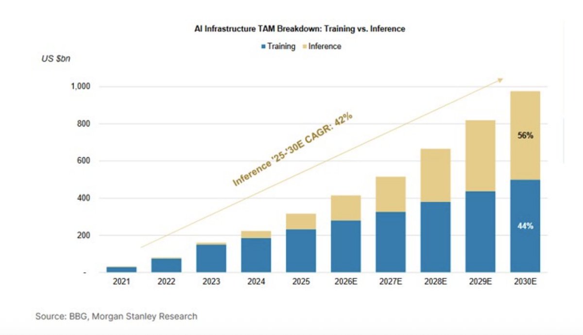
> Massive Market Growth: The total addressable market (TAM) for AI infrastructure is projected to reach nearly $1,000 billion ($1 trillion) by 2030.
> The Rise of Inference: While "Training" historically dominated early AI infrastructure spend, "Inference" is expected to grow at a blistering 42% CAGR between 2025 and 2030.
> The Pivot by 2030: By 2030, the market share is projected to flip, with Inference capturing the majority share at 56%, leaving Training at 44%.
Unprecedented Contract and Spot Pricing Mismatches
> DDR5 Pricing Surge: After a long flat period through late 2025, DDR5 prices experienced an unprecedented spike going into 2026. Spot prices surged past $45.00, while contract prices trailed tightly behind around $37.50.
> SSD (NAND) Disconnection: For 512GB PCIe 4.0 SSDs, a massive gap opened up in 2026. Interestingly, the OEM Contract price spiked dramatically higher to $118, while the Channel Spot price leveled off and dropped lower to $84.
> Inventory Normalization: Total supply-chain inventory weeks (across suppliers, PC OEMs, servers, and smartphones) peaked around mid-2024 to early-2025 and have steadily declined/normalized through 2026.
Cyclical Nature of Memory ("Rinse & Repeat")
> Predictable 4-Year Cycles: The historical data highlights clear, supply-driven memory cycles that repeat roughly every 4 years (e.g., peaks/troughs around 2010–2014, 2014–2018, 2018–2022).
> An Anomalous 2026 Spike: The current cycle moving into 2026 shows an outlier, nearly vertical surge. The DRAM Contract Year-over-Year (YoY) growth has skyrocketed to a historic high of 820%, shattering all previous cyclical peaks from the last 15 years.
$MU $NVDA $AMD $INTC $GOOGL $CBRS $AMZN
Memory storage is undergoing a frenzied production expansion, ushering semiconductor equipment into a 'super cycle'!
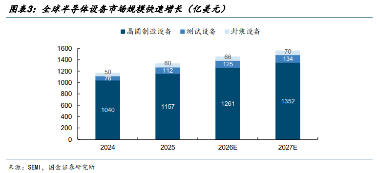
Data from SEMI reveals a strong upward trajectory for the semiconductor sector. The overall global market for semiconductor equipment is projected to climb from USD 116.6 billion in 2024 to USD 155.6 billion by 2027, growing at a steady compound annual growth rate (CAGR) of 10.1%. Within this broader expansion, testing equipment stands out for its high market elasticity. The specialized testing segment is expected to nearly double, jumping from USD 7.6 billion in 2024 to USD 13.4 billion in 2027. This rapid surge represents a much sharper CAGR of 21.1%, outpacing the wider equipment market.
Supply-side constraints are intensifying the cyclical swings of the market. Global equipment manufacturers are facing a severe squeeze from critical component shortages and maxed-out production capacity. As a result, lead times for key front-end and memory-support hardware have stretched to a massive 12 to 24 months, alongside rising prices. These shipment bottlenecks are directly delaying the expansion plans of industry giants like Samsung, SK Hynix, and Micron. However, this backlog is creating an ideal strategic window for domestic Chinese equipment suppliers. It gives them a prime opportunity to accelerate local import substitution while simultaneous
ly diversifying and expanding their global customer base.
AI servers drive up memory consumption, widening the supply-demand gap
The root cause of this equipment cycle lies in the significantly higher memory consumption of AI servers compared to traditional servers. Estimates indicate that a single AI server uses 8 to 10 times more DRAM and approximately 3 times more NAND than a conventional server.
While demand is rising, supply of general-purpose memory has not expanded in parallel. Samsung and SK Hynix have allocated 80% to 90% of their advanced-node capacity to HBM production, while Micron has redirected around 70% of its capacity toward HBM and high-end DDR5. Inventory levels at the three major memory manufacturers stand at approximately four weeks, well below the healthy safety stock range of 8 to 12 weeks. Prices have already responded accordingly. According to TrendForce, Q2 2026 contract prices for DDR5 are forecast to rise 58% to 63% quarter-over-quarter, while NAND Flash contract prices are expected to increase 70% to 75% sequentially. The HBM capacity shortfall is estimated at 50% to 60%. The memory market is also expanding. The global memory chip market was valued at USD 192.9 billion in 2024, rising to USD 289.0 billion in 2025, and is projected to reach USD 377.5 billion in 2026, with potential growth to USD 723.7 billion by 2030—a compound annual growth rate of 17.7% from 2025 to 2030.
Memory manufacturers are ramping up capacity, providing a solid foundation for equipment order fulfillment
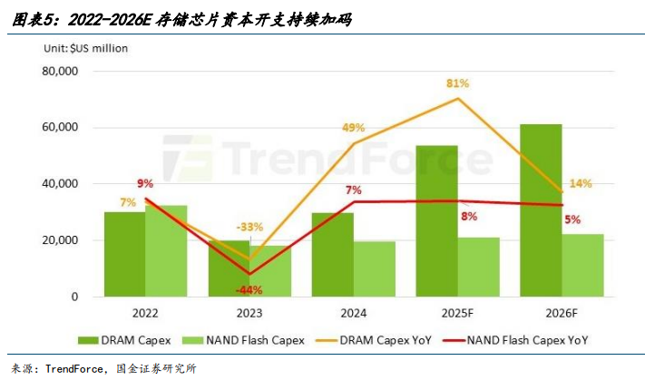
According to TrendForce data, global DRAM capital expenditure is projected to rise from USD 53.7 billion in 2025 to USD 61.3 billion in 2026, an increase of 14% year-over-year; NAND capital expenditure is expected to grow from USD 21.1 billion in 2025 to USD 22.2 billion in 2026, up 5% year-over-year. Combined capital expenditure by Samsung, SK Hynix, and Micron in 2026 is forecast to reach USD 53.5 billion, a 16% increase compared to 2025.
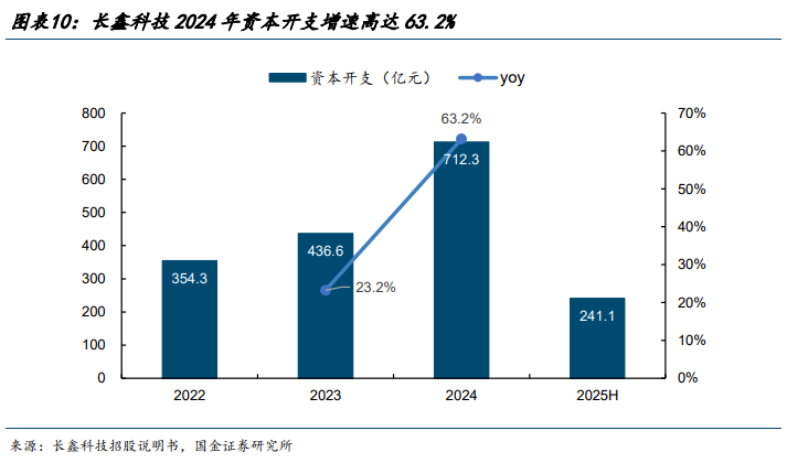
Micron is leading in capacity expansion efforts. Its planned capital expenditure for 2026 amounts to USD 27 billion, representing a 70.3% year-over-year increase. SK Hynix reported year-over-year capital expenditure growth rates of 65.8% in 2024 and 75.5% in 2025. Domestic memory manufacturers are also ramping up investments. ChangXin Technology reported revenue of RMB 24.18 billion in 2024, up 166.1% year-over-year; for the first three quarters of 2025, revenue reached RMB 32.08 billion, a 97.8% year-over-year increase. In terms of capital expenditure, ChangXin Technology invested RMB 71.23 billion in 2024, a 63.2% year-over-year increase.
Capacity expansions by ChangXin Technology and Yangtze Memory Technologies (YMTC) are driving more direct demand for domestic equipment. ChangXin Technology plans to add 50,000 to 60,000 wafers per month in monthly production capacity by 2026, corresponding to equipment procurement expenditures of approximately RMB 35–43 billion. YMTC’s Phase III project has entered the equipment installation and commissioning stage and is expected to commence large-scale mass production in the second half of 2026, with associated equipment procurement valued at around RMB 20 billion.
Extended overseas delivery timelines create a dual opportunity window for domestic equipment suppliers.
Global semiconductor component lead times have significantly lengthened in 2026. Automotive-grade 32-bit MCUs now have lead times exceeding 52 weeks, SiC components range from 25 to 40 weeks, and analog ICs range from 20 to 48 weeks. Component shortages are now adversely impacting equipment delivery schedules. Leading overseas equipment manufacturers such as Applied Materials and Tokyo Electron face constraints due to shortages of critical components and saturated production capacity, extending delivery lead times for certain equipment to 12–24 months. This presents a window of opportunity for domestic equipment vendors. Chinese manufacturers have already established product portfolios in etching, thin-film deposition, cleaning, and testing, offering clearer advantages in delivery efficiency and cost. Overseas wafer fabs, under pressure to expand capacity, are beginning to engage with domestic suppliers, with markets in South Korea and Southeast Asia emerging as potential sources of incremental demand. However, opportunities are not evenly distributed. Success in securing overseas qualifications and repeat orders ultimately depends on process stability, customer validation timelines, and delivery capability.
Domestic supply chain gaps determine where equipment flexibility lies.
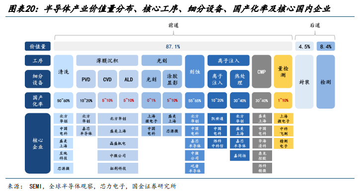
The localization rate for cleaning equipment has reached 50% to 60%, while etching equipment stands at 55% to 65%. For CMP and thermal processing, the rate is between 30% and 40%. However, it remains low in high-barrier segments: PVD at 10% to 20%, CVD/ALD and coat-develop systems each at 5% to 10%, metrology and inspection at only 1% to 10%, and lithography equipment at just 0% to 1%.
This is also why front-end metrology and back-end testing have been prioritized. Although they do not represent the largest segments by equipment volume, they constitute clearer bottlenecks with greater potential for domestic substitution.
Front-end metrology and inspection represent one of the most critical bottlenecks for domestic equipment.
Metrology and inspection equipment is used throughout the front-end wafer fabrication process to measure parameters such as film thickness, critical dimensions, and wafer surface defects. It is not merely a final quality check but an integral part of process control during lithography, etching, and thin-film deposition steps, directly affecting yield.
According to SEMI, metrology and inspection equipment accounts for approximately 13% of the global semiconductor equipment market. QYResearch data shows that the global semiconductor metrology and inspection market was valued at approximately USD 19.22 billion in 2025, is projected to reach USD 21.3 billion in 2026, and could grow to USD 32.1 billion by 2030, representing a compound annual growth rate (CAGR) of 10.8% from 2026 to 2030.
With a localization rate of only 1% to 10%, the segment remains constrained by the fact that high-precision hardware and software are dominated by overseas leaders, wafer fabs require lengthy verification cycles, customers are reluctant to switch suppliers, and export controls have further amplified supply chain uncertainty.
Once domestic manufacturers pass validation, the value of subsequent repeat orders increases. Demand for testing will rise with advancements in memory, advanced process nodes, increased 3D NAND layer counts, and advanced packaging.
The value of back-end FT testing is being repriced upward.
Testers are the core component of semiconductor test equipment. In the back-end testing equipment sector, testers account for approximately 63% of the total value, with memory testers representing about 21% of the overall tester market.
The memory test equipment market is nearly monopolized by overseas industry leaders. In 2023, Advantest held a 56% share of the global memory tester market, while Teradyne accounted for 43%, together totaling 99%. Domestic vendors have primarily entered the mid-to-low-end memory testing and ancillary equipment segments, with high-end memory ATE systems remaining a key weakness.
The importance of FT testing is increasing. CP testing occurs after wafer fabrication but before packaging and primarily screens basic electrical parameters. FT testing takes place after packaging and, in addition to verifying basic electrical parameters, also validates system-level functionality, dynamic parameters, timing characteristics, bandwidth speed, and signal integrity. FT testing imposes higher requirements on channel count, test frequency, high-speed signal processing capability, and timing precision.
Pricing also reflects this gap. International high-end FT testers are priced above RMB 11 million per unit, compared to RMB 9 million per unit for high-end CP testers. According to QYResearch, the global FT final test equipment market is projected to reach USD 3.84 billion in 2025, USD 4.1 billion in 2026, and grow to USD 5.47 billion by 2030, representing a compound annual growth rate (CAGR) of 7.5% from 2026 to 2030.
Huawei’s ‘Tao’s Law’ has further elevated the strategic value of back-end processes. Technologies such as 3D stacking, chiplets, hybrid bonding, and TSVs mean that chip performance no longer relies solely on front-end geometric scaling. As packaging and testing complexity increases, back-end equipment is no longer merely a supporting element.
J.P. Morgan: Power Semiconductor
1. Grid to Rack (20kV AC --> 800V DC)
Infineon stands out as a clear leader here, boasting the broadest portfolio and acting as the leading 1.2–3.3kV SiC MOSFET supplier, qualified by Nvidia for 800V architecture.
Navitas offers the highest voltage SiC (2.3–6.5kV) targeting SST applications.
STMicroelectronics and ON Semiconductor show strong presence with SiC portfolios, while Monolithic Power Systems (MPS) has no presence at this stage.
2. 800V DC --> 48V/12V/6V DC (Stage 1 - Inside the Rack)
Infineon and Navitas both show highly competitive GaN (Gallium Nitride) offerings. Navitas highlights a 10kW all-GaN 800V-to-50V platform achieving 98.5% peak efficiency.
Monolithic Power Systems is actively sampling 800V solutions and features integrated 48V direct-to-load modules.
Rohm is deploying its EcoGaN 650V HEMTs in AI server PSUs but has a more limited GaN breadth compared to Navitas or Infineon.
3. 48V/12V/6V to AI Chip (~1V DC) (Stage 2 - VRM / PoL)
This final stage delivers low-voltage, high-current power directly to the AI processor (GPU/ASIC) via Voltage Regulator Modules (VRM) and Point of Load (PoL).
Infineon remains dominant as the leading supplier of sub-100V MOSFETs and power stages to all major GPU makers and hyperscalers.
Monolithic Power Systems is a major force here, gaining significant share in VRM sockets and showing strength with hyperscalers for custom ASIC power delivery.
Analog Devices acts as an "intelligence layer" around the VRM, focusing on multi-phase digital controllers and monolithic smart power stages.
Rohm and STMicroelectronics have limited presence or are not significant players in this final AI chip delivery stage.
Key Suppliers:
Si MOSFET
Infineon $IFX.DE, ON Semiconductor $ON, Monolithic
Power Systems $MPS, Renesas $6723.T
Si IGBT
Infineon $IFX.DE, STMicroelectronics $STM,
Mitsubishi Electric $6503.T
SiC MOSFET
Infineon $IFX.DE, STMicroelectronics $STM, ON
Semiconductor $ON, Wolfspeed $WOLF, Rohm
$6963.T
GaN HEMT
Infineon $IFX.D, Navitas $NVTS, EPC, ON
Semiconductor $ON, Innoscience $2577.HK
Gate Driver
Infineon $IFX.DE, Texas Instruments $TXN,
STMicroelectronics $STM, ON Semiconductor $ON,
Analog Devices $ADI, Renesas $6723.T
Multi-Phase Controller
Infineon $IFX.DE, Monolithic Power Systems $MPS,
Renesas $6723.T, Analog Devices $ADI, Texas
Instruments $TXN
Power Modules/Integrated Power Stages
Infineon $IFX.DE, Texas Instruments $TXN, ON
Semiconductor $ON, Analog Devices $ADI,
Renesas $6723.T, Monolithic Power Systems $MPS
Protection/Monitoring ICs
Analog Devices $ADI, Texas Instruments $TXN,
Monolithic Power Systems $MPS, Infineon $IFX.DE, ON
Semiconductor $ON, Renesas $6723.T, Microchip
Technology $MCHP
Bernstein: Japan+China Memory Interface Chip primer
1/ The CPU is un-retiring
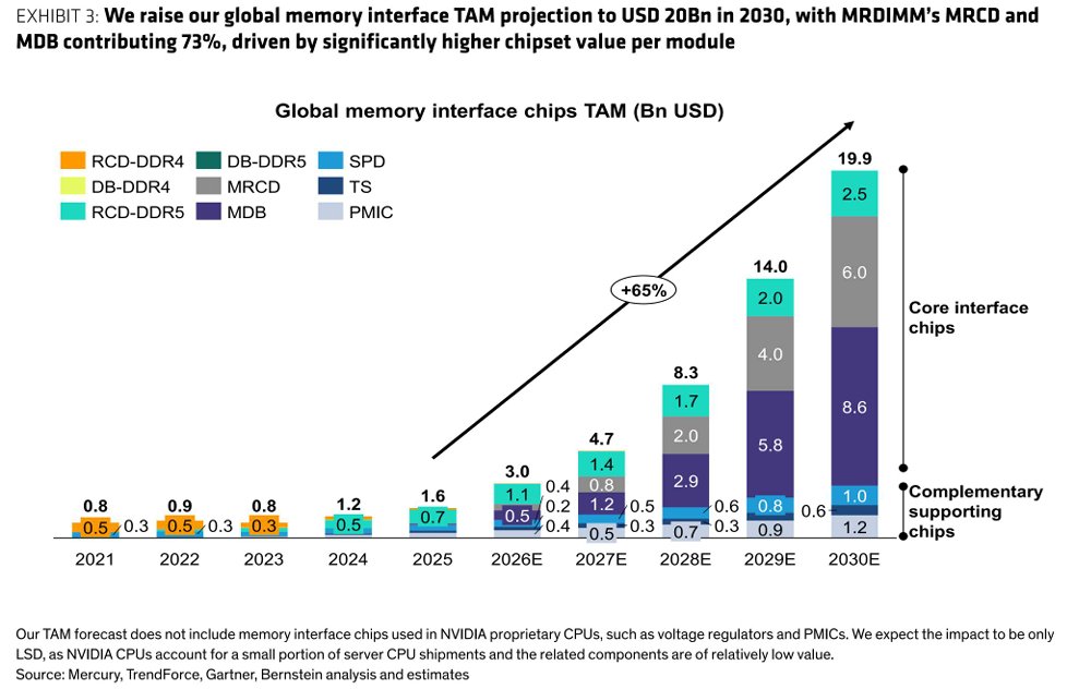
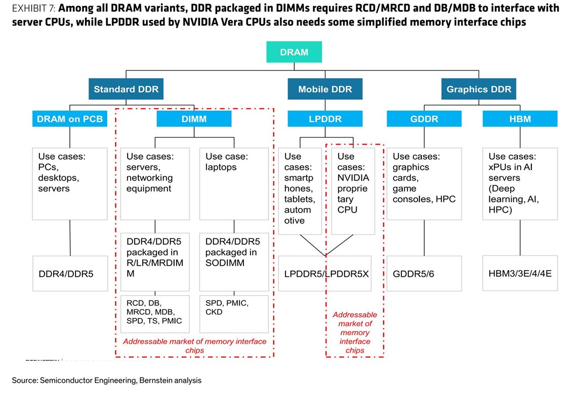
As AI shifts from GPU training to inference and agentic work, the server CPU takes back the workload, and the little chips wiring the CPU to its DRAM get paid for it. Bernstein sizes the TAM at $20bn by 2030, 65% CAGR, 3x their old number. Reiterate O on Montage and Renesas.
2/ Three drivers stacking
→ Server CPU units 30.6mn to 89.3mn by 2030, AMD just doubled its x86 server TAM to $120bn
→ More DRAM per CPU, channels going 8 to 12 to 16, AI servers filling 70-80% of slots vs ~50% on general purpose
→ More silicon per module from MRDIMM They multiply, not add. That's why the TAM grows 3x faster than CPU units.
3/ MRDIMM is the story
MRDIMM runs 1 MRCD + 10 MDB vs a single RCD on RDIMM. Content per module goes ~$7 to ~$70-80, call it 10x. Penetration 3% in 2026 to 25% by 2030 on Bernstein's math, and by 2030 MRDIMM chips are ~73% of the whole TAM. A pool that barely existed last year.
4/ This isn't LRDIMM again
The bear case is DDR4 LRDIMM had the same fat content and never cleared 1% of shipments. Difference is physics. LRDIMM added capacity nobody needed. MRDIMM doubles bandwidth past the point where RDIMM breaks down at 8800 MT/s, and both Intel and AMD are committed. Pulled by the workload, not pushed by a spec sheet.
5/ The moat is why you care
Three players, Montage ~37%, Renesas ~36%, Rambus ~20%, so ~92% of the market. Guarded by 18-24 month JEDEC qual cycles every generation, and Montage plus Renesas sit on the board writing the specs. The chip is a rounding error on module price but critical to performance, so customers pay up and never switch. Intel quit after DDR2, TI after DDR3.
6/ The supercycle helps here
Usual fear is the interface premium blocks adoption. It's the opposite. As DRAM die prices rip, the MRDIMM premium shrinks to ~10% of a 128GB RDIMM, so expensive memory actually pushes buyers toward MRDIMM. The thing scaring people about the memory cycle is the thing pulling this one forward.
7/ The value gap
Montage PT up to CNY 400 / HKD 520 from 220 / 320, 50x 2BF P/E, 27/28 EPS lifted 19% and 73%. Renesas is the sharper one. Its interface business is similar scale to Montage's while being just 6% of revenue, but its cap is only 25% above Montage's. Bernstein says management's own 20-30% CAGR guide is too low and models 42%.
8/ Right thesis, wrong entry
Not a buy today. The names ran since April, gave back 10-30% off the highs, and Bernstein expects more near-term weakness on memory sentiment, profit-taking, and substrate-shortage earnings risk for Montage and Rambus. The call is buy the dip on a 12-month view once the market starts looking at 2028.
9/ Net
Compute is sliding back to the CPU, the interface chip is the geared way to play it, and MRDIMM's 10x content jump is the durable leg. A protected oligopoly with real pricing power, the moat the humanoid names don't have. Own the dip into rising MRDIMM penetration, watch DDR6 timing as the swing factor, Renesas the mispriced one. Montage and Renesas the picks. It's actually ludicrous how much coverage I've seen for 6723 the last week.
Morgan Stanley: Memory Pricing & CapEx
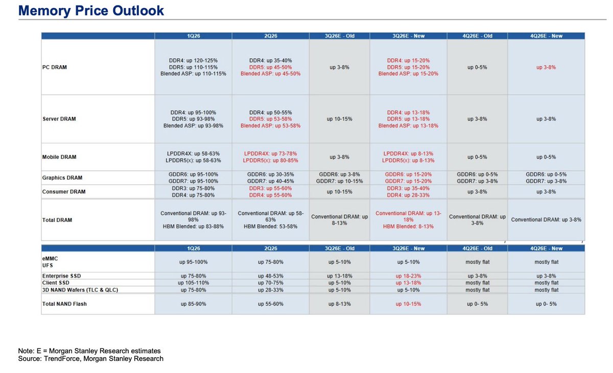
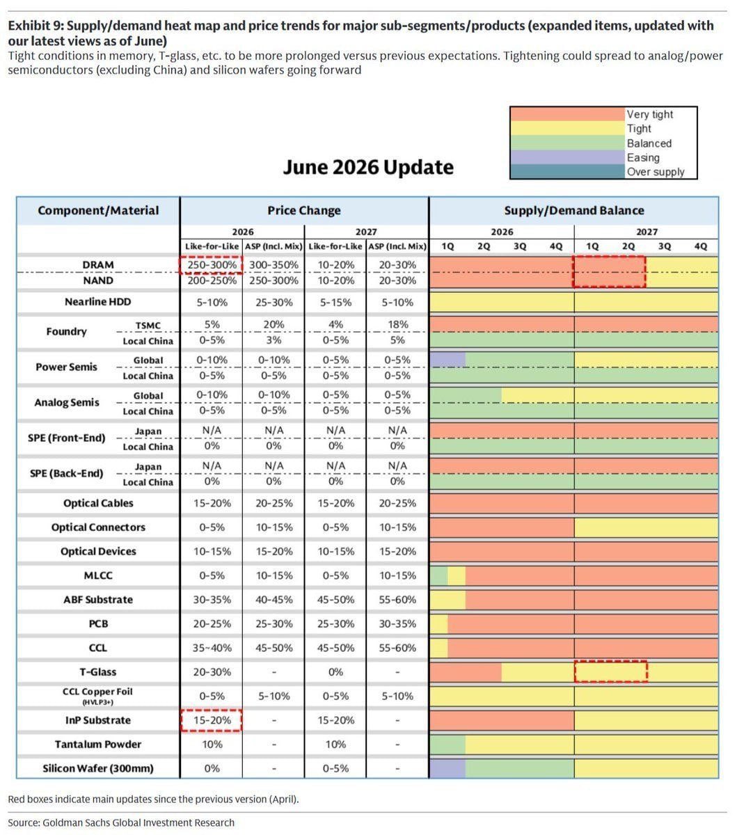
> PC & Graphics DRAM Hikes: 3Q26 estimates for PC DRAM (Blended ASP) have been revised sharply upward to up 15-20% (previously up 3-8%). Graphics DRAM (GDDR7) has also been bumped up to up 15-20% for the quarter.
> Server & HBM Tailwinds: Server DRAM Blended ASP sees an upward revision to up 13-18% in 3Q26. Crucially, HBM Blended prices are projected to rise 8-13% in 3Q26, sustaining strong pricing power.
> Enterprise SSD Outperformance: Enterprise SSD pricing shows the strongest momentum in the NAND segment, revised up to up 18-23% for 3Q26 (versus 13-18% previously). Client SSDs followed a similar upward trajectory to up 13-18%.
> 4Q26 Moderation: While 4Q26 prices are expected to lose some velocity, PC DRAM saw its 4Q projection revised up slightly to up 3-8% (from 0-5% old).
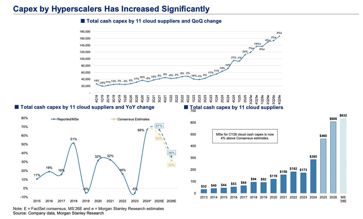
> Massive Absolute Spend: Total cash capex by the top 11 cloud suppliers is projected to reach an unprecedented $632 Billion in 2026 according to Morgan Stanley's estimates. This puts MS estimates 4% above the current FactSet consensus ($606 Billion).
BofA: AI Power Demand
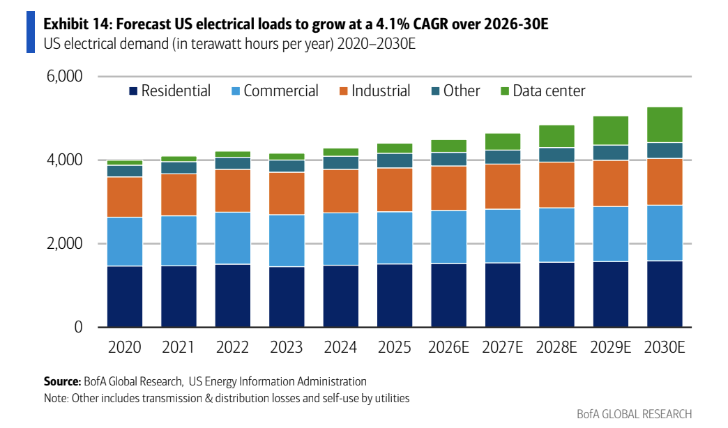
> 100+ GW Supply Gap: The US is projected to face an electricity generation shortfall of over 100 gigawatts (GW) between 2026 and 2030.
> Surging Demand vs. Capped Supply: Global semiconductor team forecasts imply a need for 230+ GW of capacity demand, while the US utilities team expects only 93 GW of accredited supply from regulated utilities.
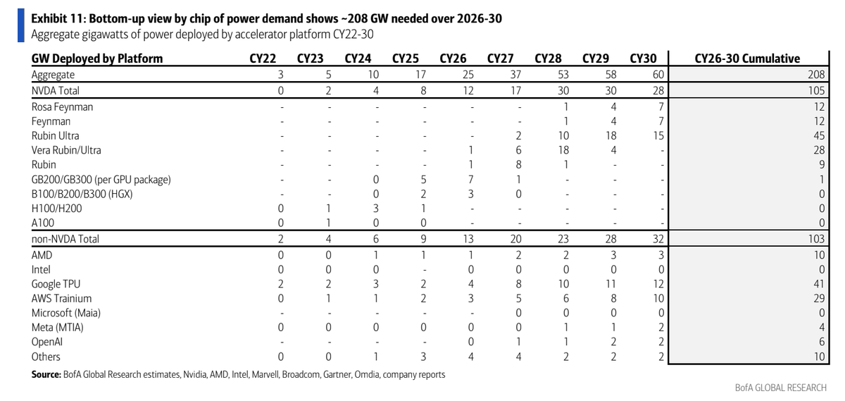
> Massive Compute Load: Driven by AI accelerators, global IT load is expected to require 208 GW between 2026 and 2030. Factoring in a 50% North American share and a 1.20 Power Usage Effectiveness (PUE) multiplier to account for cooling and facilities, this translates to 125 GW of direct US data center load growth.
> Accelerated Growth Rate: After flat growth from 2010 to 2020 (largely due to a 150bp drag from LED adoption, appliance efficiency, and residential solar), US electrical load is projected to grow at a 4.1% CAGR from 2026 to 2030.
> Rise of Gas Engines: Due to turbine scarcity and the need for fast-response grid balancing, data center developers are shifting to gas reciprocating engines. Leading manufacturers like Caterpillar, INNIO Group, Rolls Royce, and Wärtsilä have all announced capacity expansions.
> Exponential Rack-Level Power Growth: BofA Global Research pointed out a staggering leap in the power density required by Nvidia's hardware generations. Power density has jumped from 35 kilowatts (kW) per rack for the Nvidia H100 chip up to an estimated 600 kW per rack for its upcoming Feynman architecture.
$GEV $CAT $NVDA $AMD $GOOGL $AMZN $INTC