

Top Tweets for #PCBLAYOUT

💡Want to Start Learning PCB Design? Build the Right Skills First!
🌐Website: https://t.co/m2lXhNbTga
📞Contact: +91 8047112411
#PCBDesign #PCBDesignTraining #PCBLayout #ElectronicsDesign #CircuitDesign #AltiumDesigner #TechnicalTraining #ITTraining #CareerDevelopment #myTectra

🚀Build Your PCB Design Skills with myTectra!
👉Register Now: https://t.co/5IjELUlXSI
🌐https://t.co/CipN7NAzzV
#PCBDesign #PCBDesignTraining #Electronics #PCBLayout #HardwareDesign #ElectronicsEngineering #TechnicalTraining #IT #CareerSkills #myTectra #FreeTraining #FreeDemo


Join the PCB Design Training FREE DEMO by Iteanz!
👉Register: https://t.co/nJcb9259wI
🌐Course: https://t.co/5KXEBwczdD
📞 +91 8046810331
#PCBDesign #PCBDesignTraining #ElectronicsEngineering #PCBLayout #ElectronicsDesign #EngineeringJobs #TechnicalTraining #FreeDemo #Iteanz


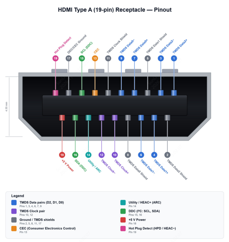
An HDMI Type A connector has 19 pins grouped into distinct signal functions, including TMDS differential pairs, DDC, CEC, HPD, and power. Understanding these pin assignments is essential for proper signal routing and impedance control.
#jlcpcb #pcblayout #HDMIPCB
CAN is a differential bus with a set impedance. So route CANH and CANL as one controlled-impedance pair, not as two ordinary digital traces.The image is for illustration purposes only. Actual routing may vary depending on the design requirements.
#jlcpcb #pcblayout #canbuspcb


The gap between #schematicgeneration and #PCBlayout reveals a larger problem: Hardware design is still organized as a serial workflow when AI agents could work from a shared system model in parallel. https://t.co/1TsEHxK62t

#murataelectronics / #psemi show off a #referencedesign for an RF #switchmatrix with a power of 12x12. I really don't want to be responsible for the #PCBlayout on this thing, though...
#orangepi bring-up time. The #hdmiadapter I used collided with the tight #pcblayout of this #singleboardcomputer - fortunately, the #proxxontools IBS came to the rescue...
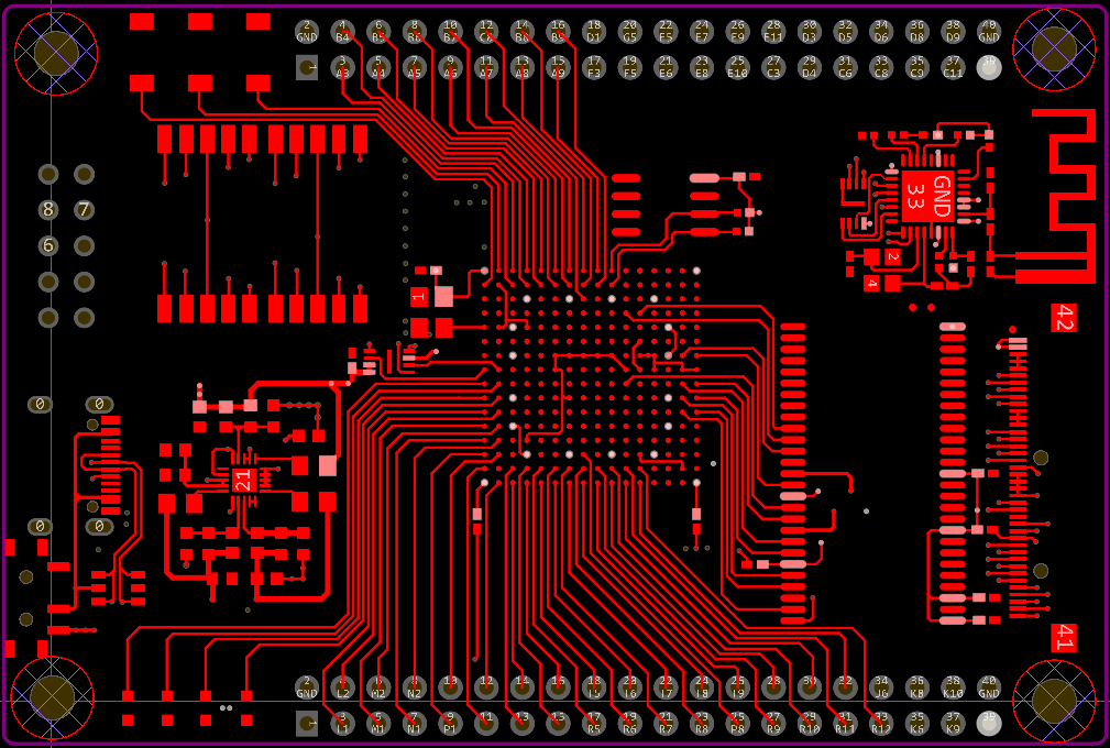
You want to swear while routing it…
Then you finish and can’t stop staring at it. 😂
That’s BGA fan-out routing.
Every trace is fighting for space.
🔴 Top | 🔵 Bottom
Which layer gave you more headaches? 👇
#PCBDesign #BGA #PCBLayout #HardwareDesign #EngineerLife #JLCPCB

#PCBdesign #lifehack. Find out how to get exact test prints out of your #PCBlayout software - these can then be used for all kinds of verification, explicitly not only for the footprints of unknown #electroniccomponents. And yes, this video still shows #target3001 which I love
Protect Your High-Speed Signal Integrity! ⚡
Don't let a misplaced resistor ruin your entire board. Upload your schematic, and our professional layout engineers will optimize your routing, curb EMI, and guarantee manufacturing readiness.
#PCBDesign #PCBLayout #JLCPCB

整然とした並列配線は、クロストークが発生するまでは見栄えが良いものです。
ノイズ。歪み。ロジックエラー。
見た目の美しいPCBも良いですが、信頼性の高いPCBの方がさらに優れています。
配線間隔を広げ、差動ペア配線を採用しましょう。ずっと簡単です。
#JLCPCB #EasyEDA #PCBLayout #Crosstalk
Why did your LVDS signal fail despite a clean DRC?
5 LVDS Layout Mistakes to Avoid:
• Crossing Ground Plane Gaps
• Skipping Length Matching
• Overusing Vias
• Routing Near Power Traces
• Ignoring Differential Impedance
#JLCPCB #PCBLayout #PCBDesign

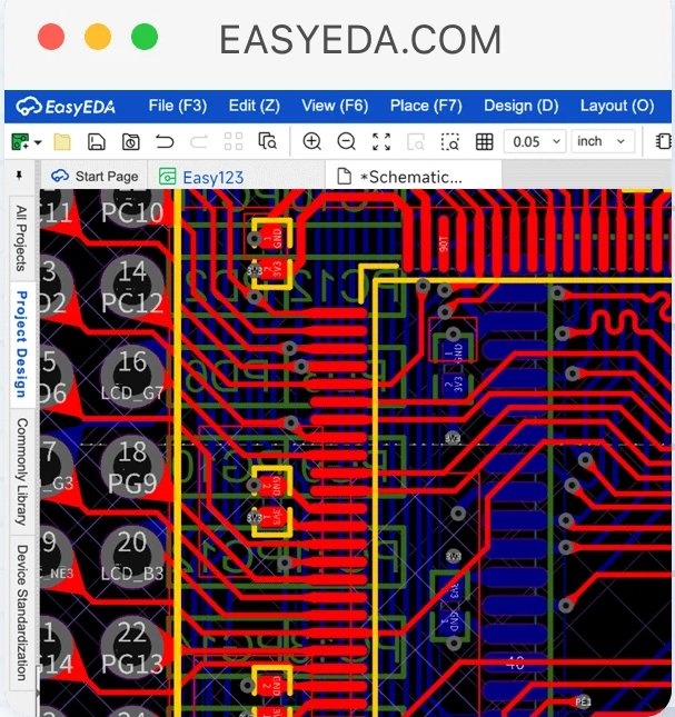
Neat parallel traces look great—until crosstalk hits.
Noise. Distortion. Logic errors.
A pretty PCB is nice. A reliable one is better.
Increase spacing + use differential-pair routing. Much easier.
#JLCPCB #EasyEDA #PCBLayout #Crosstalk #SignalIntegrity #HardwareEngineeri

Design: Masterpiece.
Placement: Tetris God.
Routing: Pure art.
DRC: 💀 103 errors.
#JLCPCB #PCBLayout #PCBDesign


Making a simple inverter 6000W, 4 transformers, sine wave, IRFz44n #PCBSync #electronic #diy #pcbmanufacturer #pcbassembly #pcbdesign #pcbdesigner #pcblayout #pcb #pcb #circuitboard
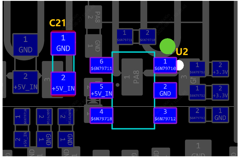
Why is this capacitor placed so close to the IC? 👀
It could sit centimeters away, but it’s right next to the power pin.
Coincidence? Nope.
What’s being minimized?
A. Voltage drop
B. Loop area / parasitic inductance
C. PCB space
D. Cost
Your answer? 👇
#JLCPCB #PCBLayout
🚨Where High Current PCB Designs Typically Fail:
❌ Undersized traces → Thermal runaway
❌ Ignored via current limit
❌ Broken ground plane → Voltage drop
❌ Relies solely on the IPC table
❌ Overlooked connector/terminal resistance
#JLCPCB #PCBLayout #PCBDesign

Finished your schematic but dreading the PCB layout process?
JLCPCB layout engineers can help you with:
1️⃣ Expert Review & Quotation
2️⃣ Component Placement
3️⃣ PCB Routing
4️⃣ Delivery Files
#JLCPCB #PCBLayout #PCBDesign

Don't let bad placement ruin your PCB signal integrity. 3 placement mistakes: ❌ Misplaced decoupling caps 📷 Connector signals crossing functional zones 📷 #PCBLayout #PCBDesign

Last Seen Hashtags on Sotwe
Most Popular Users

Elon Musk 
@elonmusk
241.3M followers

Barack Obama
@barackobama
118.8M followers

Cristiano Ronaldo
@cristiano
114.5M followers

Donald J. Trump
@realdonaldtrump
111.9M followers

Narendra Modi
@narendramodi
107M followers

Rihanna
@rihanna
98.7M followers

NASA
@nasa
92.3M followers

Justin Bieber
@justinbieber
91.8M followers

KATY PERRY
@katyperry
90M followers

Taylor Swift
@taylorswift13
84M followers

Lady Gaga
@ladygaga
75.5M followers

Virat Kohli
@imvkohli
73.4M followers

Kim Kardashian
@kimkardashian
70.8M followers

YouTube
@youtube
68.7M followers

Neymar Jr
@neymarjr
66.4M followers

Bill Gates
@billgates
65.2M followers

Selena Gomez
@selenagomez
63.1M followers

The Ellen Show
@theellenshow
62.2M followers

CNN
@cnn
61.7M followers

X
@x
60.6M followers