

Top Tweets for #Semiconductorvaluechain

#Semiconductorvaluechain
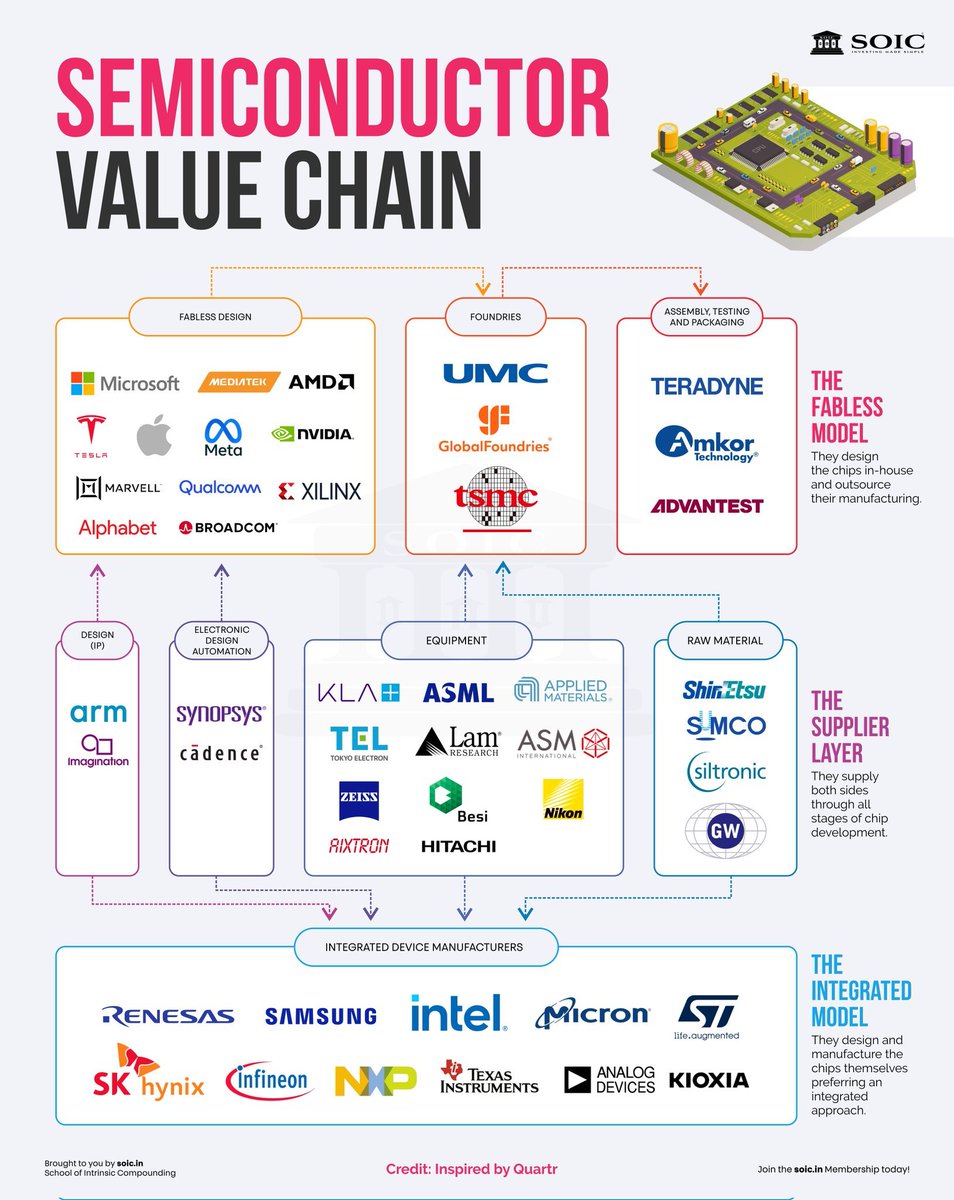
Understanding the Semiconductor Value Chain: An Investor’s Ecosystem Playbook
Sand to Silicon: The Journey of a Microchip
Every day, you use a smartphone that calculates billions of operations in a split second. But did you know your phone's brain—the microchip—starts its life as ordinary desert sand?
Turning a handful of sand into a smart device requires pushing human technology to its absolute limit. Today, that high-tech journey is moving closer to home. Driven by a massive ₹76,000 Crore ($10 Billion) government push, India is rapidly building its own semiconductor ecosystem from scratch.
Why India’s Electronics Market is Exploding 🚀
Before looking at the factory floor, it helps to understand the massive forces driving this tech boom. India is riding a major long-term growth wave powered by three key pillars:
The India Semiconductor Mission (ISM): A massive ₹76,000 Crore ($10 Billion) government piggy bank. The state uses this money to pay for up to 50% of the heavy setup costs whenever a company builds a new chip factory or packaging plant in the country.
Production-Linked Incentive (PLI) Schemes: Over ₹1,47,000 Crore ($17+ Billion) in cash rewards deployed by the government. Tech brands get paid extra bonuses simply for manufacturing smartphones, laptops, and circuit boards locally in India rather than importing them.
The "China+1" Global Shift: Major global tech giants (like Apple and its partners) are actively trying to diversify their manufacturing networks so they do not rely entirely on a single country. India is stepping up as the primary alternative hub for this international investment capital.
Let's look at the four steps that turn sand into smart tech, along with the Indian companies leading the charge:
Step 1: From Desert Sand to Mirror-Polished Wafers
Ordinary sand is melted down and highly purified into flawless silicon logs. These logs are then sliced into paper-thin, mirror-like disks called wafers, which serve as the foundation for microchips.
Financial Economics (TAM & Capex)
>>Global Segment TAM: ₹1,17,600 Crore ($14 Billion).
>>Minimum Setup Capex (Per Facility): ₹1,680 Crore to ₹4,200 Crore ($200M – $500M). Building a wafer slicing and ingot pulling plant requires major capital for precision diamond wire saws, automated edge-grinders, and high-temperature furnace controls.
>>Global Leaders: Shin-Etsu (Japan), Sumco (Japan), GlobalWafers (Taiwan), Siltronic (Germany).
>>Indian Pioneer to Watch: Raana Semiconductors is working on indigenous CZ-based crystal growth and silicon ingot processing setups.
>>Investor Insight: Raw wafer production remains the most heavily imported step in the domestic pipeline. As the ISM begins rolled-out support for raw chemical refinement, early-stage quartz miners, industrial gas refiners, and chemical players will see long-term structural demand.
Step 2: Front-End Fabrication (The Foundry)
Using light and chemicals, microscopic circuit patterns and billions of tiny switches are printed onto the wafers. Tiny copper wires are then layered on top to connect them all into working microchips.
Financial Economics (TAM & Capex)
>> Global Segment TAM: ₹9,24,000 Crore ($110 Billion).
>> Minimum Setup Capex (Per Facility): ₹42,000 Crore to ₹1,26,000 Crore ($5 Billion – $15 Billion). Foundries represent one of the most capital-intensive industrial installations in human history. A single advanced EUV photolithography scanner from ASML costs over ₹1,600 Crore ($200M), and a fab requires multiple units alongside complex Class 1 cleanroom filtration systems.
>>Global Leaders: TSMC (Taiwan), Intel (USA), Samsung Foundry (South Korea).
>>Indian Pioneers to Watch:
--> Tata Electronics / PSMC JV: Constructing India's landmark ₹91,000 Crore commercial 300mm chip fab in Dholera, Gujarat, targeting legacy and foundational nodes to supply the automotive, power, and consumer electronics spaces.
--> Suchi Semicon: Building foundational chip foundry and micro-assembly manufacturing footprints.
>> Investor Insight: Front-end fabs are highly capital-intensive projects with multi-year gestation periods. The primary investment theme here is ecosystem infrastructure. Companies providing specialized industrial engineering, cleanroom construction, high-purity water systems, and infrastructure logistics are the first to capture cash flows as these mega-fabs break ground.
Step 3: Back-End Packaging & Testing (ATMP / OSAT)
The wafers are sliced with diamond saws into individual chip squares, which are wired onto a base. Each chip is then sealed in a protective black plastic shell and tested under real electrical stress.
Financial Economics (TAM & Capex)
>>Global Segment TAM: ₹3,78,000 Crore ($45 Billion).
>>Minimum Setup Capex (Per Facility): ₹840 Crore to ₹4,200 Crore ($100M – $500M). Packaging facilities are asset-heavy but feature a fraction of the entry costs required by foundries. Capital is deployed into high-speed automated dicing saws, wire-bonding machines, transfer molding presses, and expensive automated test equipment (ATE).
>>Global Leaders: ASE Group (Taiwan), Amkor Technology (USA), JCET (China), SPIL (Taiwan).
>>Indian Players to Watch:
--> CG Power / Renesas JV: Establishing a high-reliability semiconductor assembly ecosystem backed by Murugappa Group's industrial scale.
--> Kaynes Semicon (Subsidiary of Kaynes Technology): Constructing a state-of-the-art mass packaging unit in Sanand, Gujarat, targeting specialized industrial power modules and advanced systems-in-package.
--> Sahasra Semiconductors: Operating India's first active commercial memory packaging plant in Bhiwadi, Rajasthan, exporting finished MicroSD cards and flash arrays globally.
>> Investor Insight: This is the near-term sweet spot for public equity investors. OSAT facilities require significantly less capital expenditure than frontend fabs and reach operational profitability much faster. Companies like Kaynes Technology and CG Power are leveraging strong baseline industrial earnings to cross-fund these high-margin semiconductor ventures, creating an appealing value inflection point on their balance sheets.
Step 4: Circuit Board Assembly (PCBA / SMT)
Robots precisely place the sealed chips onto a fiberglass board using metal paste, which is baked in an oven to permanently melt them into place. The completed circuit board is inspected and built into the final device shell.
Financial Economics (TAM & Capex)
>> Global Segment TAM: ₹46,200 Crore ($5.5 Billion) for advanced defense, space, and high-performance computing boards; stretching past ₹46,20,000 Crore ($550B+) for mass consumer electronic product assemblies.
>> Minimum Setup Capex (Per SMT Line): ₹15 Crore to ₹45 Crore ($2M – $5M) per line. This is a scalable, modular capacity business model. A firm can start with 2 SMT lines (comprising solder printers, high-speed chip shooters, and reflow ovens) and add more lines as customer volume expands.
>> Global Leaders: Foxconn (Taiwan), Pegatron (Taiwan), Jabil (USA), Flex (Singapore).
>> Indian Powerhouses to Watch:
--> Dixon Technologies: The undisputed market leader in domestic high-volume consumer assembly, populating motherboards for global smartphone, notebook, and smart TV brands under multiple PLI umbrellas.
--> Kaynes Technology: The premium player for complex, high-reliability PCBAs serving defense, aerospace, and electric vehicle powertrain segments.
--> Syrma SGS Technology & Avalon Technologies: Design-led EMS specialists capturing high-margin industrial computing, healthcare systems, and global export channels.
>> Investor Insight: The Indian Electronics Manufacturing Services (EMS) layer is experiencing an explosive revenue boom. Driven by localized sourcing mandates under the IT Hardware PLI 2.0, assembly giants are moving from low-margin contract work into high-margin complex component manufacturing. Look for players showing an expanding mix of high-layered PCBAs and proprietary intellectual property, as they will capture significant operating leverage as the domestic supply chain matures.
The Investor’s Ecosystem Playbook
The Indian semiconductor narrative is no longer a distant policy concept—it is a live capital deployment cycle. From an investment perspective, the value chain behaves in distinct waves based on Capex realities and project timelines:
[Wave 1: Capital Projects]
Infrastructure & SMT Equipment
Capex: ₹15C–₹45C per SMT line
(Immediate Cash Flows)
[Wave 2: OSAT Scaling]
Kaynes, CG Power, Sahasra
Capex: ₹840C–₹4,200C per plant
(12–24 Month Earnings)
[Wave 3: Mega Fabs]
Tata Electronics / PSMC
Capex: ₹42,000C+ per Fab
Capex: ₹42,000C+ per Fab
The combination of clear policy directions under the ISM and billions of dollars in private capital deployment has set the stage for major transformations. As these components come together over the coming years, India's electronic ecosystem is well-positioned to evolve from an assembly hub into a core architecture pioneer on the global stage.
[Not investment advice, DYOR]
![ramesh_vd's tweet photo. #Semiconductorvaluechain
Understanding the Semiconductor Value Chain: An Investor’s Ecosystem Playbook
Sand to Silicon: The Journey of a Microchip
Every day, you use a smartphone that calculates billions of operations in a split second. But did you know your phone's brain—the microchip—starts its life as ordinary desert sand?
Turning a handful of sand into a smart device requires pushing human technology to its absolute limit. Today, that high-tech journey is moving closer to home. Driven by a massive ₹76,000 Crore ($10 Billion) government push, India is rapidly building its own semiconductor ecosystem from scratch.
Why India’s Electronics Market is Exploding 🚀
Before looking at the factory floor, it helps to understand the massive forces driving this tech boom. India is riding a major long-term growth wave powered by three key pillars:
The India Semiconductor Mission (ISM): A massive ₹76,000 Crore ($10 Billion) government piggy bank. The state uses this money to pay for up to 50% of the heavy setup costs whenever a company builds a new chip factory or packaging plant in the country.
Production-Linked Incentive (PLI) Schemes: Over ₹1,47,000 Crore ($17+ Billion) in cash rewards deployed by the government. Tech brands get paid extra bonuses simply for manufacturing smartphones, laptops, and circuit boards locally in India rather than importing them.
The "China+1" Global Shift: Major global tech giants (like Apple and its partners) are actively trying to diversify their manufacturing networks so they do not rely entirely on a single country. India is stepping up as the primary alternative hub for this international investment capital.
Let's look at the four steps that turn sand into smart tech, along with the Indian companies leading the charge:
Step 1: From Desert Sand to Mirror-Polished Wafers
Ordinary sand is melted down and highly purified into flawless silicon logs. These logs are then sliced into paper-thin, mirror-like disks called wafers, which serve as the foundation for microchips.
Financial Economics (TAM & Capex)
>>Global Segment TAM: ₹1,17,600 Crore ($14 Billion).
>>Minimum Setup Capex (Per Facility): ₹1,680 Crore to ₹4,200 Crore ($200M – $500M). Building a wafer slicing and ingot pulling plant requires major capital for precision diamond wire saws, automated edge-grinders, and high-temperature furnace controls.
>>Global Leaders: Shin-Etsu (Japan), Sumco (Japan), GlobalWafers (Taiwan), Siltronic (Germany).
>>Indian Pioneer to Watch: Raana Semiconductors is working on indigenous CZ-based crystal growth and silicon ingot processing setups.
>>Investor Insight: Raw wafer production remains the most heavily imported step in the domestic pipeline. As the ISM begins rolled-out support for raw chemical refinement, early-stage quartz miners, industrial gas refiners, and chemical players will see long-term structural demand.
Step 2: Front-End Fabrication (The Foundry)
Using light and chemicals, microscopic circuit patterns and billions of tiny switches are printed onto the wafers. Tiny copper wires are then layered on top to connect them all into working microchips.
Financial Economics (TAM & Capex)
>> Global Segment TAM: ₹9,24,000 Crore ($110 Billion).
>> Minimum Setup Capex (Per Facility): ₹42,000 Crore to ₹1,26,000 Crore ($5 Billion – $15 Billion). Foundries represent one of the most capital-intensive industrial installations in human history. A single advanced EUV photolithography scanner from ASML costs over ₹1,600 Crore ($200M), and a fab requires multiple units alongside complex Class 1 cleanroom filtration systems.
>>Global Leaders: TSMC (Taiwan), Intel (USA), Samsung Foundry (South Korea).
>>Indian Pioneers to Watch:
--> Tata Electronics / PSMC JV: Constructing India's landmark ₹91,000 Crore commercial 300mm chip fab in Dholera, Gujarat, targeting legacy and foundational nodes to supply the automotive, power, and consumer electronics spaces.
--> Suchi Semicon: Building foundational chip foundry and micro-assembly manufacturing footprints.
>> Investor Insight: Front-end fabs are highly capital-intensive projects with multi-year gestation periods. The primary investment theme here is ecosystem infrastructure. Companies providing specialized industrial engineering, cleanroom construction, high-purity water systems, and infrastructure logistics are the first to capture cash flows as these mega-fabs break ground.
Step 3: Back-End Packaging & Testing (ATMP / OSAT)
The wafers are sliced with diamond saws into individual chip squares, which are wired onto a base. Each chip is then sealed in a protective black plastic shell and tested under real electrical stress.
Financial Economics (TAM & Capex)
>>Global Segment TAM: ₹3,78,000 Crore ($45 Billion).
>>Minimum Setup Capex (Per Facility): ₹840 Crore to ₹4,200 Crore ($100M – $500M). Packaging facilities are asset-heavy but feature a fraction of the entry costs required by foundries. Capital is deployed into high-speed automated dicing saws, wire-bonding machines, transfer molding presses, and expensive automated test equipment (ATE).
>>Global Leaders: ASE Group (Taiwan), Amkor Technology (USA), JCET (China), SPIL (Taiwan).
>>Indian Players to Watch:
--> CG Power / Renesas JV: Establishing a high-reliability semiconductor assembly ecosystem backed by Murugappa Group's industrial scale.
--> Kaynes Semicon (Subsidiary of Kaynes Technology): Constructing a state-of-the-art mass packaging unit in Sanand, Gujarat, targeting specialized industrial power modules and advanced systems-in-package.
--> Sahasra Semiconductors: Operating India's first active commercial memory packaging plant in Bhiwadi, Rajasthan, exporting finished MicroSD cards and flash arrays globally.
>> Investor Insight: This is the near-term sweet spot for public equity investors. OSAT facilities require significantly less capital expenditure than frontend fabs and reach operational profitability much faster. Companies like Kaynes Technology and CG Power are leveraging strong baseline industrial earnings to cross-fund these high-margin semiconductor ventures, creating an appealing value inflection point on their balance sheets.
Step 4: Circuit Board Assembly (PCBA / SMT)
Robots precisely place the sealed chips onto a fiberglass board using metal paste, which is baked in an oven to permanently melt them into place. The completed circuit board is inspected and built into the final device shell.
Financial Economics (TAM & Capex)
>> Global Segment TAM: ₹46,200 Crore ($5.5 Billion) for advanced defense, space, and high-performance computing boards; stretching past ₹46,20,000 Crore ($550B+) for mass consumer electronic product assemblies.
>> Minimum Setup Capex (Per SMT Line): ₹15 Crore to ₹45 Crore ($2M – $5M) per line. This is a scalable, modular capacity business model. A firm can start with 2 SMT lines (comprising solder printers, high-speed chip shooters, and reflow ovens) and add more lines as customer volume expands.
>> Global Leaders: Foxconn (Taiwan), Pegatron (Taiwan), Jabil (USA), Flex (Singapore).
>> Indian Powerhouses to Watch:
--> Dixon Technologies: The undisputed market leader in domestic high-volume consumer assembly, populating motherboards for global smartphone, notebook, and smart TV brands under multiple PLI umbrellas.
--> Kaynes Technology: The premium player for complex, high-reliability PCBAs serving defense, aerospace, and electric vehicle powertrain segments.
--> Syrma SGS Technology & Avalon Technologies: Design-led EMS specialists capturing high-margin industrial computing, healthcare systems, and global export channels.
>> Investor Insight: The Indian Electronics Manufacturing Services (EMS) layer is experiencing an explosive revenue boom. Driven by localized sourcing mandates under the IT Hardware PLI 2.0, assembly giants are moving from low-margin contract work into high-margin complex component manufacturing. Look for players showing an expanding mix of high-layered PCBAs and proprietary intellectual property, as they will capture significant operating leverage as the domestic supply chain matures.
The Investor’s Ecosystem Playbook
The Indian semiconductor narrative is no longer a distant policy concept—it is a live capital deployment cycle. From an investment perspective, the value chain behaves in distinct waves based on Capex realities and project timelines:
[Wave 1: Capital Projects]
Infrastructure & SMT Equipment
Capex: ₹15C–₹45C per SMT line
(Immediate Cash Flows)
[Wave 2: OSAT Scaling]
Kaynes, CG Power, Sahasra
Capex: ₹840C–₹4,200C per plant
(12–24 Month Earnings)
[Wave 3: Mega Fabs]
Tata Electronics / PSMC
Capex: ₹42,000C+ per Fab
Capex: ₹42,000C+ per Fab
The combination of clear policy directions under the ISM and billions of dollars in private capital deployment has set the stage for major transformations. As these components come together over the coming years, India's electronic ecosystem is well-positioned to evolve from an assembly hub into a core architecture pioneer on the global stage.
[Not investment advice, DYOR]](https://pbs.twimg.com/media/HMXf-vxb0AAg__g.jpg)

#SemiconductorValueChain at #JewarAirport
⬛ UP government should focus on establishing a Semiconductor Value Chain near Jewar Airport
⬛ Don't waste valuable land for real estate development.

Australia Taiwan relations have entered a new chapter with 🇦🇺’s largest semiconductor company @MorseMicro launching its new TW office. This will expand business links & bring Australian innovation & expertise in WiFi Halow chips into Taiwan & the region. #semiconductorvaluechain

Last Seen Hashtags on Sotwe
monkeyapp video*
Seen from Algeria
ChristmasWithCWAY
Seen from Brazil
MilitaryGroove
Seen from Argentina
sex
Seen from United States
GodEnzo
Seen from Argentina
TheCollectiveBham
Seen from United States
INDvsENG2ndT20I
Seen from United States
보이프라2
Seen from Korea
habeshagirls
Seen from Kenya
syakirah viral
Seen from Indonesia
Most Popular Users

Elon Musk 
@elonmusk
240.9M followers

Barack Obama
@barackobama
119.2M followers

Donald J. Trump
@realdonaldtrump
111.8M followers

Cristiano Ronaldo
@cristiano
111.6M followers

Narendra Modi
@narendramodi
107M followers

Rihanna
@rihanna
97.9M followers

NASA
@nasa
92.2M followers

Justin Bieber
@justinbieber
91.1M followers

KATY PERRY
@katyperry
88.2M followers

Taylor Swift
@taylorswift13
82.1M followers

Lady Gaga
@ladygaga
73.6M followers

Virat Kohli
@imvkohli
70.8M followers

Kim Kardashian
@kimkardashian
70M followers

YouTube
@youtube
68.7M followers

Bill Gates
@billgates
64.2M followers

Neymar Jr
@neymarjr
63.6M followers

The Ellen Show
@theellenshow
62.4M followers

CNN
@cnn
61.8M followers

Selena Gomez
@selenagomez
61.3M followers

X
@x
60.8M followers