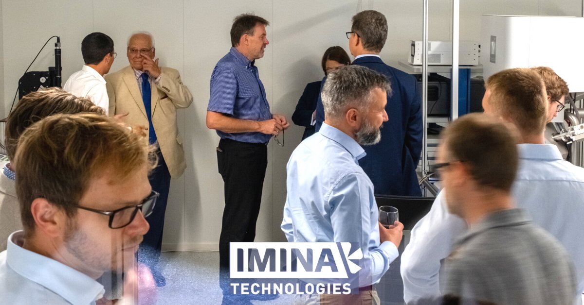
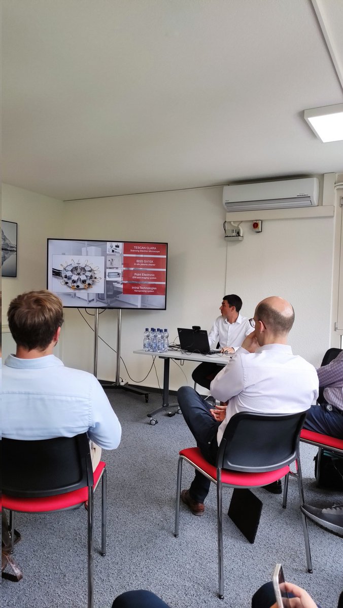
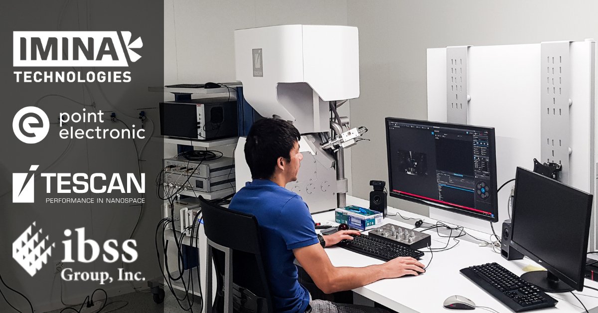
Great workshop to celebrate our new demo lab! Thanks to the participants from @ST_World, @Presse_IMWS, @tescan_micro, point electronic and IBSS Group and to the online attendees.
Check out our next hybrid workshop in Singapore: https://t.co/Ay4a5wyyEN
We are opening a new demo/service lab at our HQ!
Celebrate the occasion with us - join an online workshop on #nanoprobing/#EFA with excellent speakers from #Semiconductorindustry and a live demo.
When: June 28th, at 13:30 CEST.
Program & registration: https://t.co/MVYXsIlLeK
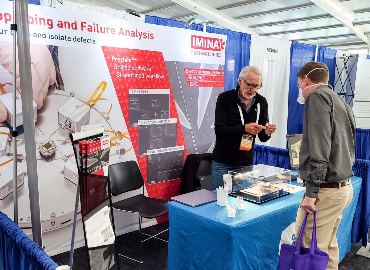
@imina_tech team had a great time at #ECTC2022 in San Diego! Our #insitu#SEM#nanoprobing solutions have enjoyed a lot of attention from the participants.
Special thanks to the organizers @IEEEorg and our partner Angstrom Scientific for their support!
https://t.co/moUJOBn1II
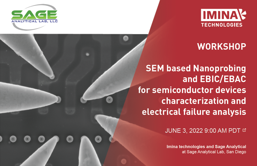
Are you in San Diego? Don’t miss our upcoming workshop at @SageFALab! It is a rare chance to see a live #nanoprobing & #EFA demo with your own eyes.
Where: Sage Analytical Lab
When: June 3rd, 9 am PDT
Register for free: https://t.co/WQJBIVDYKr
#failureanalysis#semiconductors
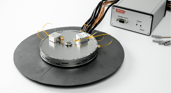
Meet our new product: Thermal Stage for temperature-dependent #Nanoprobing and Electrical Failure Analysis.
The stage operates in the range from -30°C to 150°C, reaching the target temperature within minutes.
#semiconductors#AcademicTwitter
https://t.co/SRRv4wrG2v
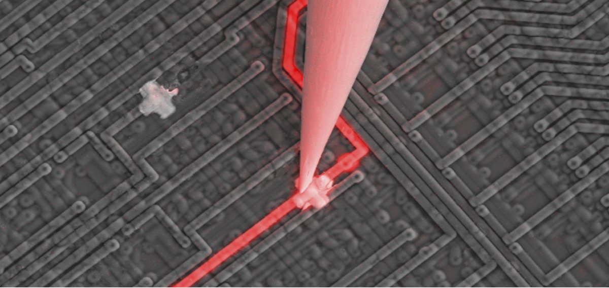
Do you know why our #Nanoprobing solution with EFA module is the best-in-class #ElectricalFailureAnalysis tool?
The answer is simple: no defect will remain hidden.
A longer answer can be found here: https://t.co/tg4D0T9zkl
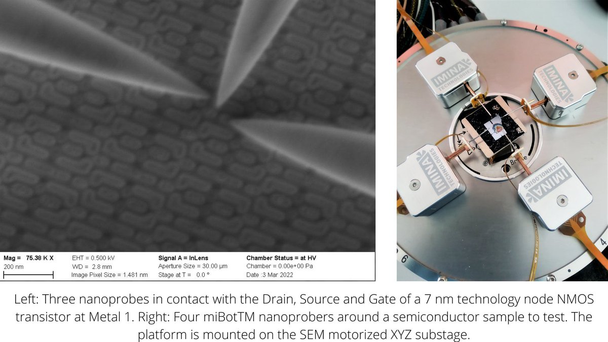
#Nanoprobing on small technology nodes such as #7nm technology is a tricky task. Check out out latest application note to discover how our #NANO solution can be used for such measurements—and optimizing the #workflow!
https://t.co/I8IQVAYpTg
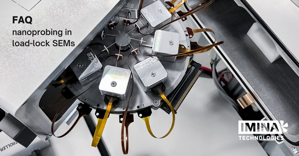
Is @imina_tech#nanoprobing platform compatible with a load-lock SEM?
Yes.
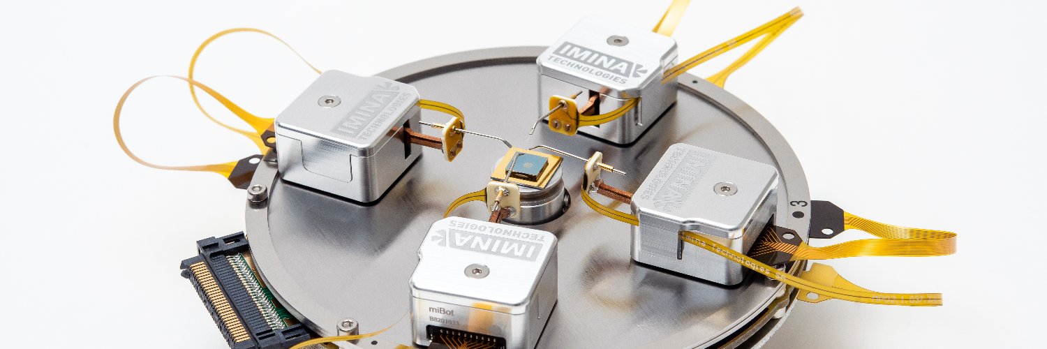
Our load-lock platform comes in two sizes that fit up to 4 or 8 robots and it does not affect SEM operation when the nanoprobers are not in use.
More details:
https://t.co/XTWiWeGUrY
#Physics#phdchat
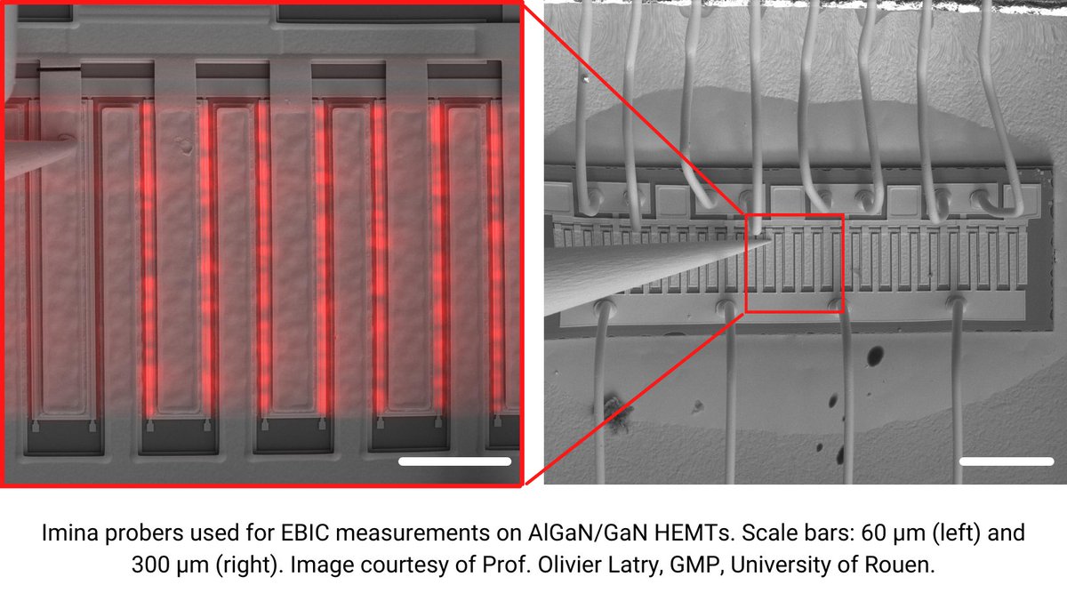
“It took us just two training sessions to master #nanoprobing and #EBIC. It is really easy to land miBots’ tips.”—says Prof. Olivier LATRY who leads the study on improving #HEMT (high electron mobility transistors) #reliability at GMP Rouen.
Read more at https://t.co/NarAJRQ0nh
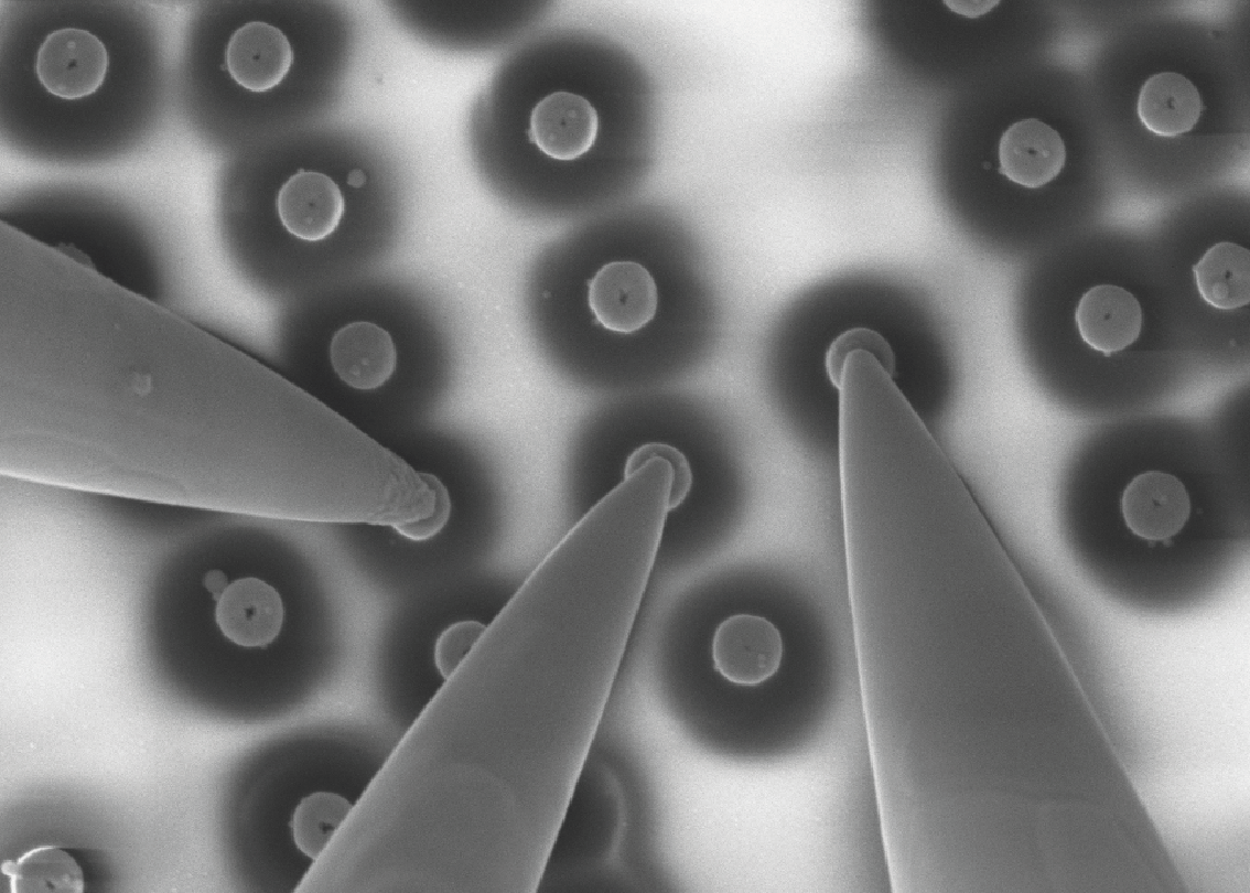
Can we tilt our #nanoprobing platform?
Precisely landing probes and maintaining steady electrical contacts while the setup is tilted can be tricky.
Our nanoprobers can securely hold onto the platform at tilts up to 55° and be used for #circuitediting https://t.co/8kA2t1HBAj
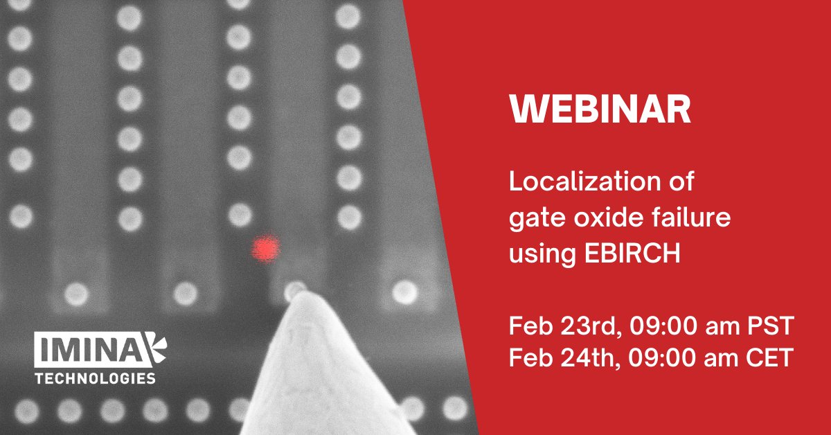
A new webinar dedicated to #EBIRCH technique!
This webinar will include a live demo of EBIRCH performed in-situ with our #nanoprobing
solution and point electronic acquisition system.
Register for free: https://t.co/knd7ln2w6C
#failureanalysis#transistors#semiconductors
Do you need to characterize many identical #devices across a sample? Our XYZ sub-stage accelerates the #workflow by moving the sample independently from the probes. This way, you don't need to realign the #probing tips each time you go to the next device.
https://t.co/8UFPoHanTM
Check our latest application note on #FemtoFarad Capacitance-Voltage measurement at #Transistor Contact Level. We show how to measure #capacitance down to 2.5fF with the noise around 50 aF!
https://t.co/T0nSYMnxhK