Protect innovation in Illinois. The Illinois State Senate is currently reviewing SB 1797, a bill that could hinder innovation and place excessive regulations on legitimate digital asset companies. https://t.co/BmpXsqpptm
For anyone out there who thinks your vote doesn't matter, let Jeanie be an example to all of us of the power of your vote. Don't take your vote, or your voice, for granted. Happy 104th birthday, Jeanie! https://t.co/t887H7j2Rw
Enough delays, @UnitedHealthGRP! It's time to stop finding new ways to cause delays for #IBD patients needing treatment and sit down with the @CrohnsColitisFn to come up with patient-centric solutions. @UHC#noUHCdelays
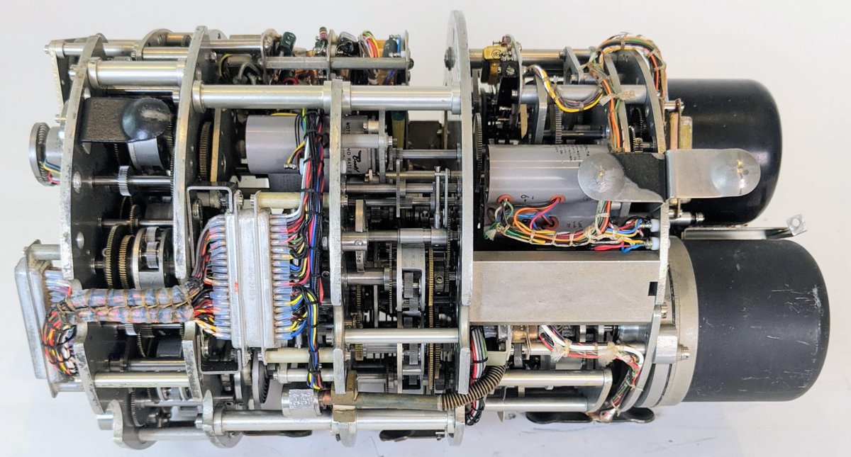
How did fighter planes in the 1950s perform calculations before compact digital computers were available? With the Bendix Central Air Data Computer! This electromechanical analog computer used gears and cams to compute "air data" for fighter planes such as the F-101. 1/13
Registration for Hacktoberfest 2023 is now live! Link your GitHub or GitLab account and get your profile ready to go to track your pull/merge requests on October 1st. https://t.co/DMBXO3ASBF
MicroZed Chronicles: Outputting Clocks.
We all know that if we want to get the best performance, we should place input clocks to our FPGAs on clock capable or dedicated clock pins.. When it comes to generating output clocks from an FPGA though, it’s not as simple as just outputting the clock on a IO pin to get the best performance .
To give us the best performance (e.g., lowest jitter, best duty cycle and timing performance) when working with Source Synchronous Outputs (SSO), we need to use a clock forwarding approach.
In a clock forwarding approach, we leverage the IO structure provided by AMD FPGAs, more specifically the Output Double Data Register (ODDR). The ODDR outputs data on both edges of the clock, and as a result, we can set the D1 input high and D2 input low. These are then output on every clock edge, creating an output clock at the frequency of the ODDR clock.
We can demonstrate this is working as expected by creating a simple test bench for the clock output module.
Most importantly, this ensures we keep the clock on global clocking resources, which we can observe by looking at the implementation view.
Zooming in allows you to see the ODDR register as it is described in the RTL.
By using the ODDR for clock forwarding, and the associated data leveraging IO flip flops the clock and data are aligned. As the delay through the ODDR and the IO flip flops is designed to be identical. As a result, the delays will be balanced against each other, providing better timing performance.
If we updated the design to remove the ODDR and simply output the clock and reimplement the design, we will see the ODDR bypassed and the global clock buffer being connected directly to the output pin. This uses local routing which results in more skew and jitter on the output clock signal. It will also contribute to the overall clock performance metrics and impact the overall device timing closure.
This means that the receiving device has to declare a larger clock uncertainty because the jitter is larger. If this is another FPGA, for example, it can make achieving timing closure more challenging.
When it comes to constraining the forward clock, we can use timing wizard to define the forward clock constraint or we can enter it by hand in the XDC file. When using the timing wizard, both create generated clock and forward clock constraints pages and result in the same type of constraint being created.
create_generated_clock -name clk_out1 -source [get_pins design_1_i/clk_output_0/U0/ODDR_inst/C] -divide_by 1 [get_ports clk_out1]
There are also a number of steps we can take to achieve the lowest jitter outside of clock forwarding. The first step is to use the PLL instead of the MMCM. To reduce the jitter on the clock, we should also try to physically and temporally separate it from potential noise sources.
Physically, we can try to isolate the clock pins from other signals (especially single-ended signals) which we can do by creating virtual grounds around the clock output. We can achieve a virtual ground during the design of the circuit board and FPGA by assigning the IO bank pins to drive out a logic low. Those pins are then connected to ground on the PCB design.
If, temporally, we are using the same clock internally then we should be using a different clock phase. The exact phase might vary from design to design, but we can see the impacts of using a particular clock phase by monitoring the VCCint ripple / bounce with the clocks set at different phases.
If you follow these clock forwarding rules, hopefully you’ll be able to increase performance when working with source synchronous outputs.
#FPGA


![ATaylorFPGA's tweet photo. MicroZed Chronicles: Outputting Clocks.
We all know that if we want to get the best performance, we should place input clocks to our FPGAs on clock capable or dedicated clock pins.. When it comes to generating output clocks from an FPGA though, it’s not as simple as just outputting the clock on a IO pin to get the best performance .
To give us the best performance (e.g., lowest jitter, best duty cycle and timing performance) when working with Source Synchronous Outputs (SSO), we need to use a clock forwarding approach.
In a clock forwarding approach, we leverage the IO structure provided by AMD FPGAs, more specifically the Output Double Data Register (ODDR). The ODDR outputs data on both edges of the clock, and as a result, we can set the D1 input high and D2 input low. These are then output on every clock edge, creating an output clock at the frequency of the ODDR clock.
We can demonstrate this is working as expected by creating a simple test bench for the clock output module.
Most importantly, this ensures we keep the clock on global clocking resources, which we can observe by looking at the implementation view.
Zooming in allows you to see the ODDR register as it is described in the RTL.
By using the ODDR for clock forwarding, and the associated data leveraging IO flip flops the clock and data are aligned. As the delay through the ODDR and the IO flip flops is designed to be identical. As a result, the delays will be balanced against each other, providing better timing performance.
If we updated the design to remove the ODDR and simply output the clock and reimplement the design, we will see the ODDR bypassed and the global clock buffer being connected directly to the output pin. This uses local routing which results in more skew and jitter on the output clock signal. It will also contribute to the overall clock performance metrics and impact the overall device timing closure.
This means that the receiving device has to declare a larger clock uncertainty because the jitter is larger. If this is another FPGA, for example, it can make achieving timing closure more challenging.
When it comes to constraining the forward clock, we can use timing wizard to define the forward clock constraint or we can enter it by hand in the XDC file. When using the timing wizard, both create generated clock and forward clock constraints pages and result in the same type of constraint being created.
create_generated_clock -name clk_out1 -source [get_pins design_1_i/clk_output_0/U0/ODDR_inst/C] -divide_by 1 [get_ports clk_out1]
There are also a number of steps we can take to achieve the lowest jitter outside of clock forwarding. The first step is to use the PLL instead of the MMCM. To reduce the jitter on the clock, we should also try to physically and temporally separate it from potential noise sources.
Physically, we can try to isolate the clock pins from other signals (especially single-ended signals) which we can do by creating virtual grounds around the clock output. We can achieve a virtual ground during the design of the circuit board and FPGA by assigning the IO bank pins to drive out a logic low. Those pins are then connected to ground on the PCB design.
If, temporally, we are using the same clock internally then we should be using a different clock phase. The exact phase might vary from design to design, but we can see the impacts of using a particular clock phase by monitoring the VCCint ripple / bounce with the clocks set at different phases.
If you follow these clock forwarding rules, hopefully you’ll be able to increase performance when working with source synchronous outputs.
#FPGA](https://pbs.twimg.com/media/F7BMhxWWAAAW5Dx.png)
![ATaylorFPGA's tweet photo. MicroZed Chronicles: Outputting Clocks.
We all know that if we want to get the best performance, we should place input clocks to our FPGAs on clock capable or dedicated clock pins.. When it comes to generating output clocks from an FPGA though, it’s not as simple as just outputting the clock on a IO pin to get the best performance .
To give us the best performance (e.g., lowest jitter, best duty cycle and timing performance) when working with Source Synchronous Outputs (SSO), we need to use a clock forwarding approach.
In a clock forwarding approach, we leverage the IO structure provided by AMD FPGAs, more specifically the Output Double Data Register (ODDR). The ODDR outputs data on both edges of the clock, and as a result, we can set the D1 input high and D2 input low. These are then output on every clock edge, creating an output clock at the frequency of the ODDR clock.
We can demonstrate this is working as expected by creating a simple test bench for the clock output module.
Most importantly, this ensures we keep the clock on global clocking resources, which we can observe by looking at the implementation view.
Zooming in allows you to see the ODDR register as it is described in the RTL.
By using the ODDR for clock forwarding, and the associated data leveraging IO flip flops the clock and data are aligned. As the delay through the ODDR and the IO flip flops is designed to be identical. As a result, the delays will be balanced against each other, providing better timing performance.
If we updated the design to remove the ODDR and simply output the clock and reimplement the design, we will see the ODDR bypassed and the global clock buffer being connected directly to the output pin. This uses local routing which results in more skew and jitter on the output clock signal. It will also contribute to the overall clock performance metrics and impact the overall device timing closure.
This means that the receiving device has to declare a larger clock uncertainty because the jitter is larger. If this is another FPGA, for example, it can make achieving timing closure more challenging.
When it comes to constraining the forward clock, we can use timing wizard to define the forward clock constraint or we can enter it by hand in the XDC file. When using the timing wizard, both create generated clock and forward clock constraints pages and result in the same type of constraint being created.
create_generated_clock -name clk_out1 -source [get_pins design_1_i/clk_output_0/U0/ODDR_inst/C] -divide_by 1 [get_ports clk_out1]
There are also a number of steps we can take to achieve the lowest jitter outside of clock forwarding. The first step is to use the PLL instead of the MMCM. To reduce the jitter on the clock, we should also try to physically and temporally separate it from potential noise sources.
Physically, we can try to isolate the clock pins from other signals (especially single-ended signals) which we can do by creating virtual grounds around the clock output. We can achieve a virtual ground during the design of the circuit board and FPGA by assigning the IO bank pins to drive out a logic low. Those pins are then connected to ground on the PCB design.
If, temporally, we are using the same clock internally then we should be using a different clock phase. The exact phase might vary from design to design, but we can see the impacts of using a particular clock phase by monitoring the VCCint ripple / bounce with the clocks set at different phases.
If you follow these clock forwarding rules, hopefully you’ll be able to increase performance when working with source synchronous outputs.
#FPGA](https://pbs.twimg.com/media/F7BMhw2X0AAY7Pc.png)
![ATaylorFPGA's tweet photo. MicroZed Chronicles: Outputting Clocks.
We all know that if we want to get the best performance, we should place input clocks to our FPGAs on clock capable or dedicated clock pins.. When it comes to generating output clocks from an FPGA though, it’s not as simple as just outputting the clock on a IO pin to get the best performance .
To give us the best performance (e.g., lowest jitter, best duty cycle and timing performance) when working with Source Synchronous Outputs (SSO), we need to use a clock forwarding approach.
In a clock forwarding approach, we leverage the IO structure provided by AMD FPGAs, more specifically the Output Double Data Register (ODDR). The ODDR outputs data on both edges of the clock, and as a result, we can set the D1 input high and D2 input low. These are then output on every clock edge, creating an output clock at the frequency of the ODDR clock.
We can demonstrate this is working as expected by creating a simple test bench for the clock output module.
Most importantly, this ensures we keep the clock on global clocking resources, which we can observe by looking at the implementation view.
Zooming in allows you to see the ODDR register as it is described in the RTL.
By using the ODDR for clock forwarding, and the associated data leveraging IO flip flops the clock and data are aligned. As the delay through the ODDR and the IO flip flops is designed to be identical. As a result, the delays will be balanced against each other, providing better timing performance.
If we updated the design to remove the ODDR and simply output the clock and reimplement the design, we will see the ODDR bypassed and the global clock buffer being connected directly to the output pin. This uses local routing which results in more skew and jitter on the output clock signal. It will also contribute to the overall clock performance metrics and impact the overall device timing closure.
This means that the receiving device has to declare a larger clock uncertainty because the jitter is larger. If this is another FPGA, for example, it can make achieving timing closure more challenging.
When it comes to constraining the forward clock, we can use timing wizard to define the forward clock constraint or we can enter it by hand in the XDC file. When using the timing wizard, both create generated clock and forward clock constraints pages and result in the same type of constraint being created.
create_generated_clock -name clk_out1 -source [get_pins design_1_i/clk_output_0/U0/ODDR_inst/C] -divide_by 1 [get_ports clk_out1]
There are also a number of steps we can take to achieve the lowest jitter outside of clock forwarding. The first step is to use the PLL instead of the MMCM. To reduce the jitter on the clock, we should also try to physically and temporally separate it from potential noise sources.
Physically, we can try to isolate the clock pins from other signals (especially single-ended signals) which we can do by creating virtual grounds around the clock output. We can achieve a virtual ground during the design of the circuit board and FPGA by assigning the IO bank pins to drive out a logic low. Those pins are then connected to ground on the PCB design.
If, temporally, we are using the same clock internally then we should be using a different clock phase. The exact phase might vary from design to design, but we can see the impacts of using a particular clock phase by monitoring the VCCint ripple / bounce with the clocks set at different phases.
If you follow these clock forwarding rules, hopefully you’ll be able to increase performance when working with source synchronous outputs.
#FPGA](https://pbs.twimg.com/media/F7BMhwzW8AA4f8W.png)







![ATaylorFPGA's tweet photo. MicroZed Chronicles: Outputting Clocks.
We all know that if we want to get the best performance, we should place input clocks to our FPGAs on clock capable or dedicated clock pins.. When it comes to generating output clocks from an FPGA though, it’s not as simple as just outputting the clock on a IO pin to get the best performance .
To give us the best performance (e.g., lowest jitter, best duty cycle and timing performance) when working with Source Synchronous Outputs (SSO), we need to use a clock forwarding approach.
In a clock forwarding approach, we leverage the IO structure provided by AMD FPGAs, more specifically the Output Double Data Register (ODDR). The ODDR outputs data on both edges of the clock, and as a result, we can set the D1 input high and D2 input low. These are then output on every clock edge, creating an output clock at the frequency of the ODDR clock.
We can demonstrate this is working as expected by creating a simple test bench for the clock output module.
Most importantly, this ensures we keep the clock on global clocking resources, which we can observe by looking at the implementation view.
Zooming in allows you to see the ODDR register as it is described in the RTL.
By using the ODDR for clock forwarding, and the associated data leveraging IO flip flops the clock and data are aligned. As the delay through the ODDR and the IO flip flops is designed to be identical. As a result, the delays will be balanced against each other, providing better timing performance.
If we updated the design to remove the ODDR and simply output the clock and reimplement the design, we will see the ODDR bypassed and the global clock buffer being connected directly to the output pin. This uses local routing which results in more skew and jitter on the output clock signal. It will also contribute to the overall clock performance metrics and impact the overall device timing closure.
This means that the receiving device has to declare a larger clock uncertainty because the jitter is larger. If this is another FPGA, for example, it can make achieving timing closure more challenging.
When it comes to constraining the forward clock, we can use timing wizard to define the forward clock constraint or we can enter it by hand in the XDC file. When using the timing wizard, both create generated clock and forward clock constraints pages and result in the same type of constraint being created.
create_generated_clock -name clk_out1 -source [get_pins design_1_i/clk_output_0/U0/ODDR_inst/C] -divide_by 1 [get_ports clk_out1]
There are also a number of steps we can take to achieve the lowest jitter outside of clock forwarding. The first step is to use the PLL instead of the MMCM. To reduce the jitter on the clock, we should also try to physically and temporally separate it from potential noise sources.
Physically, we can try to isolate the clock pins from other signals (especially single-ended signals) which we can do by creating virtual grounds around the clock output. We can achieve a virtual ground during the design of the circuit board and FPGA by assigning the IO bank pins to drive out a logic low. Those pins are then connected to ground on the PCB design.
If, temporally, we are using the same clock internally then we should be using a different clock phase. The exact phase might vary from design to design, but we can see the impacts of using a particular clock phase by monitoring the VCCint ripple / bounce with the clocks set at different phases.
If you follow these clock forwarding rules, hopefully you’ll be able to increase performance when working with source synchronous outputs.
#FPGA](https://pbs.twimg.com/media/F7BMhzTXcAAroEd.png)





