while you’re trading AI stocks I’m buying $ATOM Atomera Incorporated- the company that makes the actual semiconductor materials better. it’s like investing in better concrete while everyone else is flipping houses. I will either look genius or stupid, no in between
Here is the full transcription of the CC presentation:
Scott Bilbaut, President and CEO, Atomera:
Thanks, Mike, and good afternoon to everyone. In Atomera’s fourth quarter, we made great progress moving existing customers forward in our targeted segment, achieving very strong technical advancements. Commercial execution has been strong, and our new customer engagement is non-traditional areas, and new IC verticals in 2024. Today, I’ll give you an update on all of our activities as we close out our business prospects in the new year.
Technology news recently has been dominated by the rapid advancement of artificial intelligence and the associated semiconductor challenges that AI entails. From the allocation of limited GPU supply, the enormous stresses put on our energy infrastructure, and the associated surge in memory needs, Atomera’s technology is positioned to assist with each of these industry issues as we deliver materials which help relieve each pain point.
So let me start off with our recent exciting progress on Gate-All-Around transistor technology, which is the foundational architecture used in AI, CPUs, GPUs, and bleeding-edge network components. The challenges with manufacturing these next generation transistors revolves at 2 nanometer and below are widespread, and a concerted effort by the whole ecosystem of industry players is required to manufacture the next generation economically, with throughput and yield. This has been the focus of our recent announced strategic partnership with a large equipment OEM. Target customers are TSMC, Samsung, and Intel in production, and Rapidus, a new Japanese manufacturer, which is developing. Atomera’s MST technology delivers some very compelling solutions in this space, in particular for diffusion blocking. These tiny Gate-All-Around transistors require extremely high phosphorus doping levels, constrained to a very small area in the source and drain of the nanosheet.
Under these intense semiconductor manufacturing environment, it is difficult to keep these dopant atoms in their proper positions, and just a small amount of migration into the channel can severely impact performance, reliability, and yield. Atomera’s MST is uniquely well suited to hold these migrating phosphorus atoms in place. Although this MST characteristic is well proven in older technologies, implementing MST in devices that are around 2 nanometers while maintaining its efficacy is something that industry players must be validated on silicon at real-world scale, and we’ve been working hard to do so. Our target customers have been looking at 2 results to prove high volume manufacturability. First, that MST can be effectively deposited into the actual transistor structure, and second, that the diffusion blocking characteristics can be maintained at these nodes, even when the devices are scaled down further.
Obtaining these results is not straightforward and requires access to advanced structures that are not generally available, and we have expensive and frequently proprietary. But we have been able to make steady progress with the help of a Gate-All-Around customer and our strategic partner. Just in the last month, we obtained very exciting silicon results in both targeted areas, which we believe provide the definitive proof to enable MST at all four of the world’s Gate-All-Around customers in the future. Not only can MST be deposited into those structures using existing tools and standard gases, but it is far superior diffusion blocking material than those currently used by the industry. We anticipate that we will be able to implement this technology with leading industry players over the next few quarters.
Of course, we’re quite excited by these recent results since our advanced node, our Gate-All-Around business segment, has been growing nicely in revenue potential. But we’re also making convincing progress in our other customer areas, so let me provide a short update here. In DRAM, the technology roadmap is at a key inflection point, as DRAM finally follows other logic and memory architectures in making better use of the vertical dimension. We are gaining traction in emerging to enhance the performance of next generation architectures, in addition to solutions for products currently in production by the major memory suppliers. During the last few months, we have had two major silicon offerings that we’re working hard to validate, since their market potential is very high. Notably, these are both wafer-based solutions, which are easier to adopt and test, avoiding many of the integration complexities required in some of our other applications.
With the current robust market for memories, we believe our potential customers will have a generous R&D budget to pursue these ideas. Atomera is currently conducting many wafer runs with our various customers. Most of these are processing through their fabs, so we will expect more information soon. But one customer has just gotten preliminary results, which look promising. But we will get a better view when the final data is available. In about a month, if the results look good, we will be pushing for a joint development agreement and a license to advance this technology to production. In the RF SOI space, our offering is very strong, considering that it can provide performance improvements for multiple important areas, including for the RF switch and the low noise amplifier.
Because we are working with so many of the key players in this industry, including foundry and fabless suppliers, we hope to drive adoption broadly. Again, in this space, our solution can be implemented with a wafer-based solution, meaning our customers can choose to deposit it on wafers themselves before starting their full manufacturing processes, or they could leave this to us. We support wafers from a thin-epitaxial process. Our license structure supports both of these approaches. In power, we are working with some very large players to ultimately be incorporated into their product offerings. Although we had a setback with MST last year, we continue to work with them on MST solutions across multiple business units. In addition to our traditional BCD business opportunities, this quarter, we had several new internal interests emerge for power applications.
Throughout our internal analysis and modeling, we have uncovered an opportunity for MST in trench FETs, which are an important component in optimizing energy efficiency in AI data centers. Our simulations show the potential for MST to improve performance by more than 40%. We got this result after Christmas and already have a customer interested in kicking off development. Similarly, using our MST as insulation capability, we have been discussing many of MST can improve RF devices, virtualizing high-speed transistors frequently used for amplifying and switching signals in RF communication systems. Discussions are underway with a potential first customer in this application as well. In GaN, I’m happy to report that our first customer, commercial customer, has now started running wafers for GaN-on-silicon with MST technology. For many reasons, this is exciting.
This large customer can grow their own GaN wafers and manufacture electrical devices on them, which means they can move even faster than our in-house work with Sandia National Labs and Texas State. So we expect that we will actually move ahead of our own internal development efforts over the next few quarters. Second, they are exploring GaN in both RF and power technologies. These independent efforts by multiple industry and scientific partners frequently can accelerate time to revenue, which is what we’re hoping to accomplish. Last month, we announced that our GaN-on-silicon concept paper had been approved to move into the proposal stage for a project with PowerAmerica, to advance the state-of-the-art on wide bandgap materials. We announced this for a variety of reasons. First, we wanted to show the widespread interest from customers, the science community, and industrial organizations for an MST solution for GaN-on-silicon.
Indeed, we’ve already received several letters of support from multiple future customers showing interest in this solution. Second, this concept paper was our first application for outside development funding, and although the funds sought for this first effort are modest, they put us in the pathway for a variety of future material development funding opportunities, which can provide us assistance going down a path we are planning to travel anyway. By engaging in these joint development opportunities, we are promoting our technology, receiving financial assistance, and assuring a customer base all in one project. To summarize, the past few months have been an incredibly productive time in terms of technical development and the buildup of a variety of new customer opportunities that I believe will lead to business deals and announcements later this year.
Finally, as we close out 2025, let me give you a few thoughts on our accomplishments. Last year, we took our early development and simulation results on Gate-All-Around and converted it into what I now believe is our greatest company opportunity. We did that through working with a lead customer and with a strategic partner who’s also a major equipment OEM. This is a significant departure from how we’ve approached the market in the past. The industry has a long history of relying on this OEM to deliver their material solutions for their processes. So we truly believe that their influence will help us to convert our recent strong technical results to licenses and revenue. We made technical breakthroughs in our other core markets to enable clear applications like LNA for RF SOI, a new architecture for BCD, and next-gen DRAM solutions.
Using AI, our development team has gotten better results more efficiently than ever before. We kicked off a record number of wafer runs with our leading customers, initiated several new projects, and solidified the business talent on our team, which should lead to further contract announcements over the course of this year. Much of this work was done emphasizing wafer-based products, which we believe will result in faster time to revenue. In short, 2025 efforts have set us up well for commercial announcements later this year. With that, I’ll turn the call over to Frank to review our financials.
$atom #atomera Atomera Incorporated.
Feb 12 2026 Conference Call Transcript, CEO Scott.
Positive: Scott opens with appreciation and momentum
Confident: Scott speaks with operational authority and technical command
Forward-Looking / Expectant: Strong anticipation of growth
Strategic and Big Picture: Scott zooms out to industry transformation
For the first time, and I have been in since 2020, Scott feels like a leader who believes in the company's position, understands the technical landscape deeply, is preparing stakeholders for acceleration, and wants investors to feel the inevitability, simultaneously.
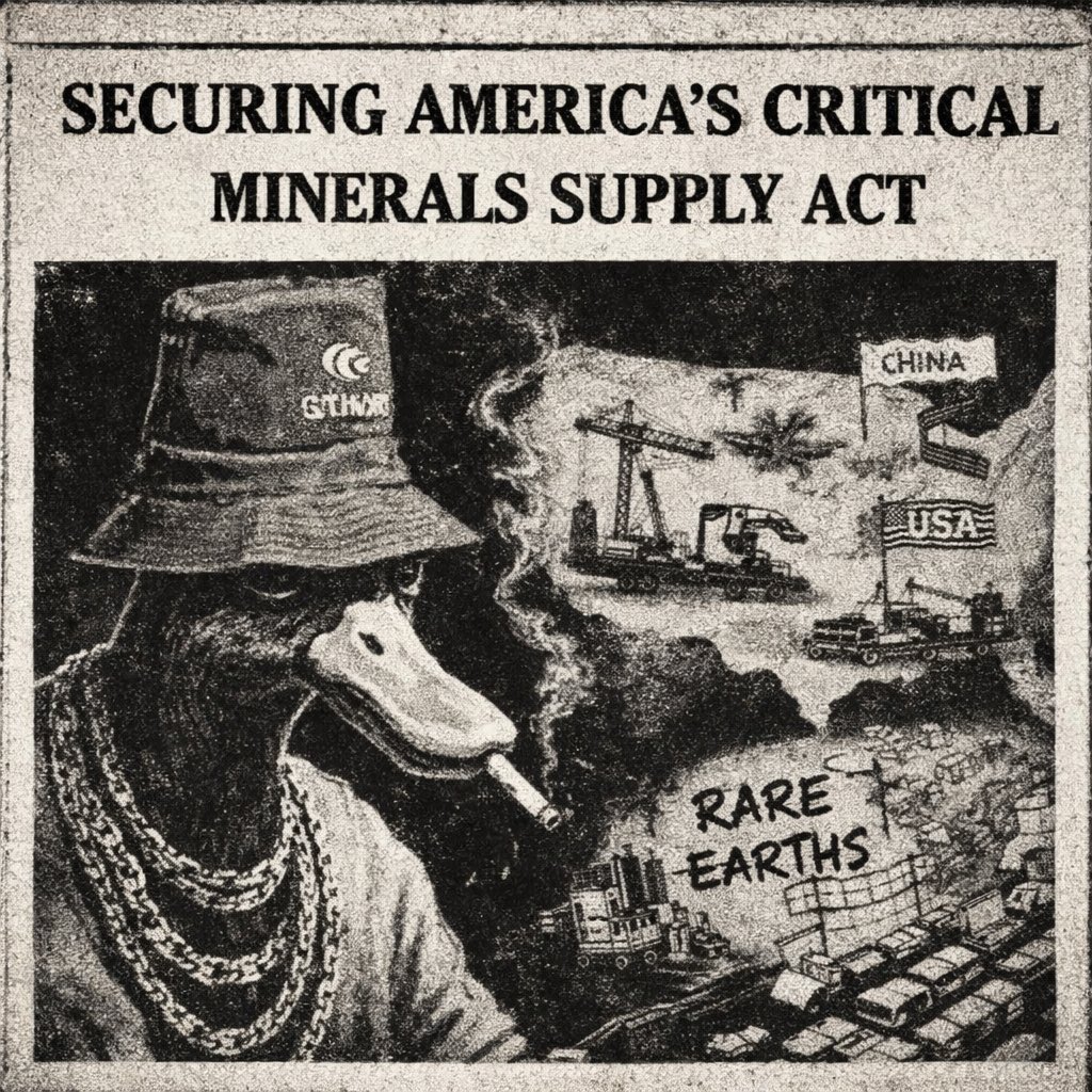
BREAKING: House Passes The Securing America’s Critical Minerals Supply Act $MP $UUUU $USAR $UAMY $AREC $TMC $UURAF
Today, Chairman Brett Guthrie and Congressman John James announced House passage of key Energy and Commerce legislation designed to fortify America’s energy supply chains, curb dependence on adversarial nations, and protect the critical resources that underpin our economy and national security.
H.R. 3617, titled “Securing America’s Critical Minerals Supply Act” requires the Department of Energy to assess critical energy resource supply chains, including critical minerals and rare earth elements, and to strengthen supply chains that are vulnerable to disruption or overreliance on adversarial nations.
By taking a holistic view of critical energy resources, the Department of Energy can identify vulnerabilities and address supply chain disruptions to help ensure Americans have access to affordable, reliable, and secure energy systems.
Lawmakers emphasized that critical minerals and rare earths are foundational to grid infrastructure, advanced manufacturing, defense systems, and next-generation technologies. Despite abundant domestic resources, the United States remains heavily import-dependent.
Source: https://t.co/ecVNhIClOs
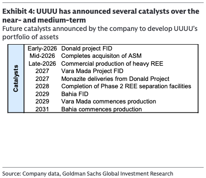
Goldman on $UUUU
"initiating coverage of UUUU with a Buy rating and a $30, 12-month price target implying 32% upside from current levels"
"UUUU owns and operates the highest-grade uranium deposit in the US as well as the White Mesa Mill, which is a key competitive advantage for the company as it is the only processing facility in the US that is able to process both uranium and rare earth elements"
"UUUU has spent over a decade assembling a broad portfolio of assets to establish itself as a leading producer of both rare earths and uranium"
"UUUU owns and operates several world-class assets across its three business units – uranium, rare earths, and heavy mineral sands"
Sprott Uranium Miners ETF ( $URNM) Explained
URNM is a pure play uranium ETF that tracks the North Shore Global Uranium Mining Index.
It focuses on companies with at least 50% of assets in uranium mining, exploration, development, production, physical uranium, or royalties.
Top holdings (approx % of fund)
Cameco Corp 20%
Uranium Energy Corp 14%
Sprott Physical Uranium Trust 12%
Energy Fuels Inc 5.5%
Paladin Energy 5.1%
Denison Mines 5.0%
Deep Yellow 4.9%
NexGen Energy 4.7%
Kazatomprom 4.5%
CGN Mining 4.3%
Why it matters
Gives diversified exposure across uranium miners, developers, explorers, and physical uranium, instead of betting on a single stock.
Direct way to express a long term view on nuclear energy growth and tightening uranium supply.
@PeterSchiff@saylor “That’s my quant. He doesn’t even speak English.”
You need one of those Peter, before you post your math.
You averaged the cost basis but didn’t average the time basis.
Scam maths.
BREAKING: After the release of an ad that caused Trump's tantrum ending trade talks with Canada, the original video of Ronald Reagan slamming tariffs has resurfaced. He called the new ad "fake."
The original destroys Trump on tariffs.
Share this widely.
A new Bitcoin giant just launched with 42,000 BTC on day one.
Backed by SoftBank, Tether and Cantor Fitzgerald.
And it’s taking direct aim at MicroStrategy.
But this isn’t just a new stock ticker.
It’s a global alliance with deep incentives to accumulate Bitcoin at scale...🧵
1. Once you realize you’re going the wrong way, turn around ASAP.
2. When you find yourself in a deep hole, the first thing to do is stop digging.
3. .....
99.99% of people are underestimating $MSTR's financial strength.
With BTC @ $79K, $MSTR holds $33.5 Billion in NET assets (assets - debt).
$33.5 Billion
Most people can't comprehend a Billion dollars.
Let alone 33 Billion.
1 Billion is One Thousand Millions.
33 Billion is Thirty Three Thousand Millions
Here's some perspective. $33B in assets alone would be ranked the 255th largest US company. Sitting between companies such as Hershey, Kraft, Robinhood, Block, and Prudential Life.
2x The size of Reddit
3x The size of GameStop
5x The size of MGM Resorts
It would also represent the 4th largest reinsurance entity on the planet, behind Lloyd's of London. (ranked by assets)
Financial strength allows for strong trading relationships, trust, and more confidence in the underwriting of future debt transactions.
_______________________
Many people have also expressed concern about $MSTR's ability to pay the $150M annual interest payment on their current preferred offerings; however, fail to recognize the scale of the interest obligation is a pittance compared to the balance sheet's net assets.
150M relative to 33,000 Million of unencumbered financial strength. (0.4%)
$MSTR's financial strength allows for ULTIMATE financial flexibility, and future debt based trading relationships (rolling the debt in different formats).
_________________________
Looking into the future, at a Bitcoin price of $180,000, $MSTR will have more unencumbered "Net Capital" Than the largest publicly traded insurance company ( $UNH), currently valued at a $480B market cap. ASSUMING ZERO additional BTC yield between now and $180K per BTC.
__________________________
In summary:
Many are vastly underestimating this strength.
We have never seen a company accumulate so much financial strength this quickly. Hard to conceptualize what hasn't existed before.
🟩👆
The 10Y Note Yield just:
1. Convinced Trump to delay tariffs by 90-days
2. Made the Fed ready to "stabilize" markets if needed
3. Made Trump ready for a phone call with Xi
4. Became one of Secretary Bessent's top priorities
5. Unwound the $800+ billion basis trade
The bond market is the new driver of economic policy.
🦔 Hey guys, I want to explain the carry trade because I think Michael is on to something and regular investors should understand it.
The "carry trade" is pretty simple at its core. For decades, people have borrowed money in Japan at super low interest rates (near zero) and then invested that money elsewhere for higher returns. Think of it like taking out a 1% loan and investing it in something that pays 5% - you pocket the difference.
This strategy has been HUGE...we're talking trillions of dollars. Hedge funds, banks, and other big players have all been doing it.
But now something's changing. Japan finally raised interest rates after keeping them near zero for 17 years. The Yen is getting stronger. And suddenly, all those investors who borrowed in Yen need to sell their investments to pay back those loans.
This creates forced selling across all kinds of assets - stocks, bonds, real estate, you name it. And it happens regardless of whether the investments themselves are good or bad.
I think this might explain a lot of the crazy market moves we've been seeing, especially in the Treasury market where yields spiked dramatically earlier this week.
While everyone's focused on Trump's tariffs (which are important!), this Japan situation could be the bigger issue lurking beneath the surface.
I hope that helps and brings some clarity 🤗