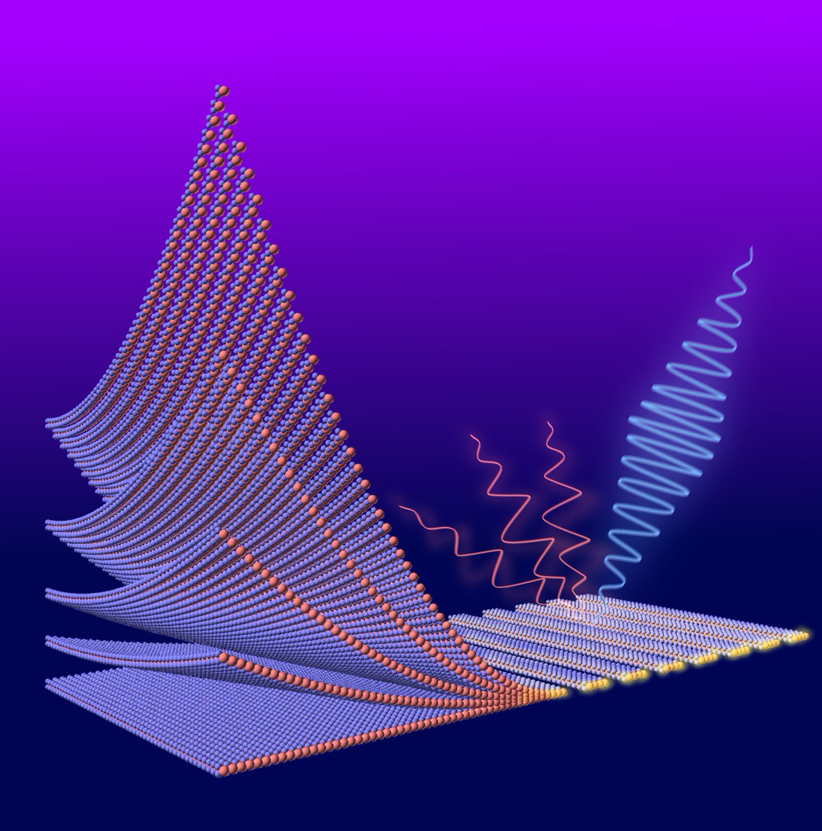
🧡Scientists from @physics_UW and partners have trapped infrared light in a layer just 40 nm thick using MoSe₂! This breakthrough could accelerate the future of photonics. he results were published in the prestigious journal “ACS Nano”
https://t.co/jr03a6ZU6p
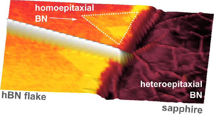
Great epitaxy,
"Using both faces of polar semiconductor wafers for functional devices", L. Deurzen, E. Kim, N. Pieczulewski, Z. Zhang, A. Feduniewicz-Zmuda, M. Chlipala, M. Siekacz, D. Muller, H. Grace Xing, D. Jena & H. Turski, Nature (2024). https://t.co/JCZZ10GrQW
MOCVD, MBE, and electrical-contacts to our monolayers: Large-Area Growth of High-Optical-Quality MoSe2/hBN Heterostructures with Tunable Charge Carrier Concentration | K. Ludwiczak et al., ACS Applied Materials & Interfaces 2024, https://t.co/YavoRrC24u
It was great to measure the electron diffraction of CVD MoSe₂ in our MBE and contribute to the study "Twisted MoSe₂ Homobilayer Behaving as a Heterobilayer" by Arka Karmakar et al., published in Nano Letters 2024.
https://t.co/7K4pTsKeX6
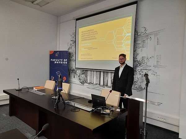
Dr. Michał Grzybowski, congratulations on the NCN Sonata project to be carried out at the Faculty of Physics, University of Warsaw. We look forward to growing together many epitaxial samples with #Altermagnetism.
Logo of our LUMS group painted! With a fluorescent paint! Today it has been hung in the corridor of @physics_UW. Here in a photo with its author, @kepolczynska.
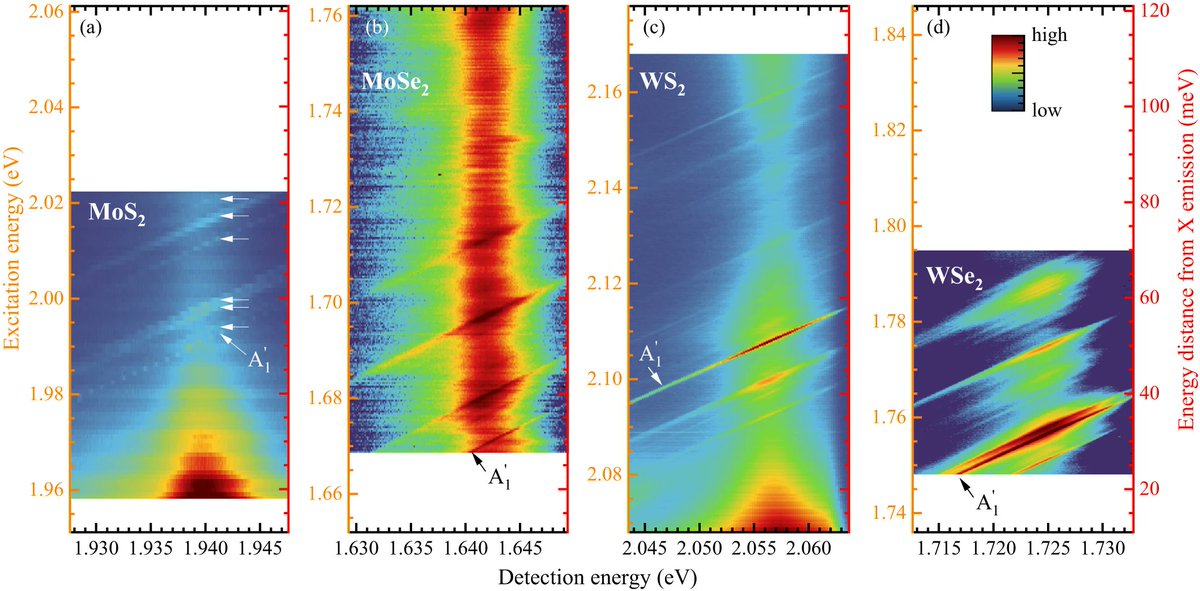
"Raman scattering excitation in monolayers of semiconducting transition metal dichalcogenides",
M. Zinkiewicz et al., npj 2D Materials and Applications 8, 2 (2024). https://t.co/L6NbIugjJd
MBE epilayers are in SI, https://t.co/NEnujvGpPp
Congratulations to Aleksander Bogucki for successfully defending his PhD thesis "The influence of strain on magnetic ion relaxation time in semiconductor nanostructures" and for receiving distinction!
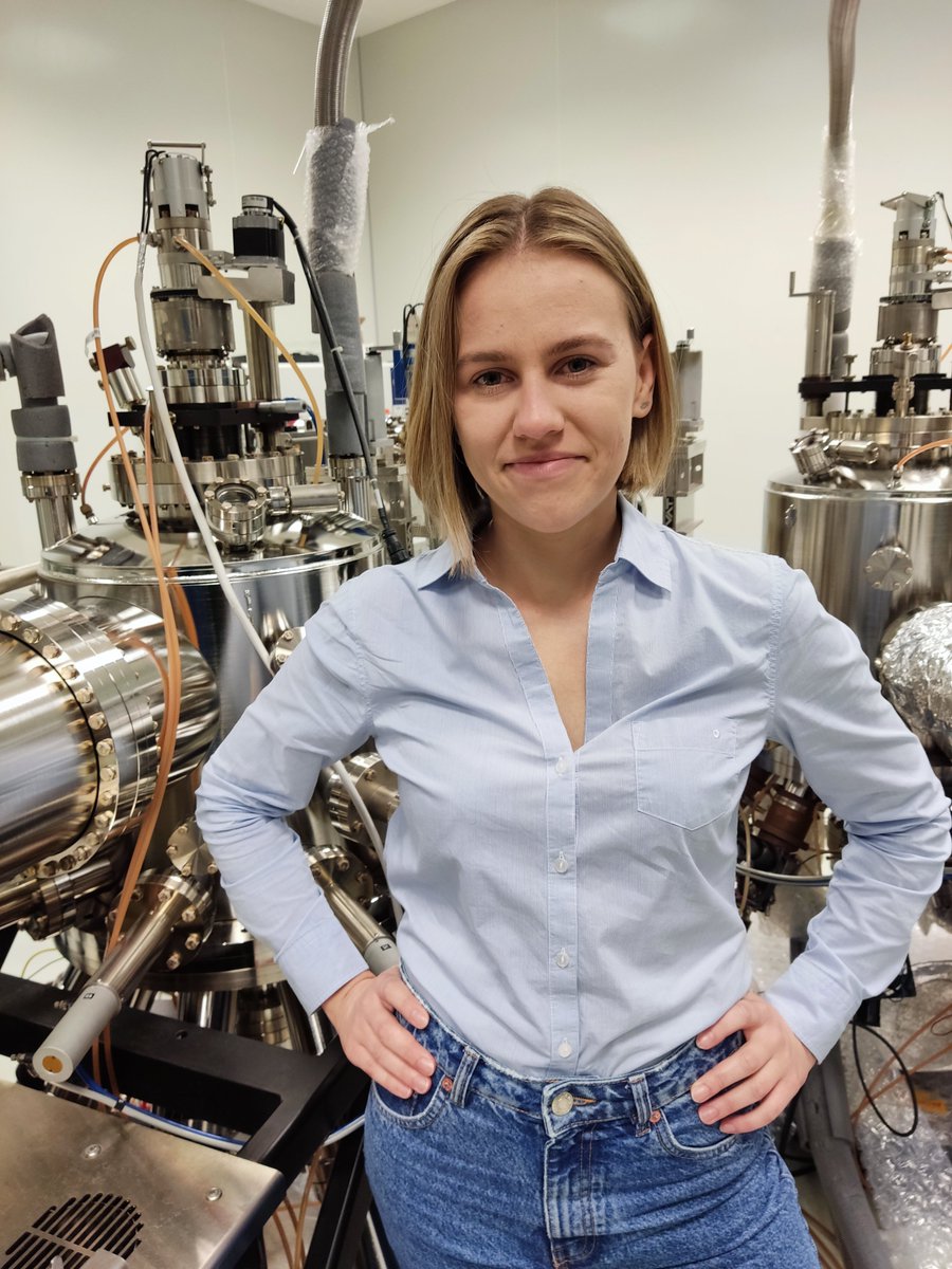
Congratulations to Julia Kucharek for NCN Preludium grant "The effects of doping and alloying on Molecular Beam Epitaxy-GrownTransition Metal Dichalcogenides"