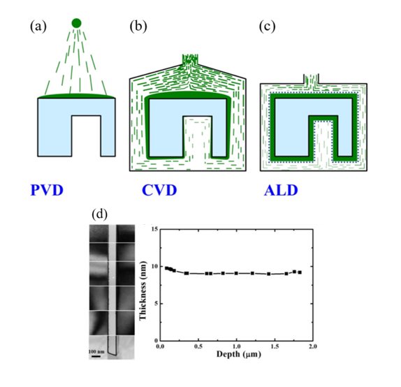
Why is ALD so important? How does it differ from CVD and PVD?
One of the key characteristics of ALD is atomic layer deposition, a thin-film process that grows materials one layer at a time. You can imagine it like snowfall—when only one layer of snowflakes falls at a time, the deposition becomes extremely uniform with excellent coverage. ALD enables deposition along edges, and even at the bottom, sides, or top surfaces, layer by layer.
In contrast, PVD (Physical Vapor Deposition) is a form of “line-of-sight deposition.” Like an arrow, it can only travel in a straight path, meaning it cannot turn corners or reach the bottom and sidewalls. As a result, PVD has very limited step coverage and can only deposit in one direction.
CVD (Chemical Vapor Deposition) is more similar to ALD, but instead of depositing one atomic layer at a time, it deposits multiple atomic layers per cycle. While CVD provides some coverage and can reach recessed areas, it is not as precise as ALD. In particular, when it comes to achieving exact control at specific locations (such as bottoms or corners), CVD falls short. Although it is faster, its precision cannot match that of ALD.
Esto se debería de aplicar en tu ciudad?
Conductores de camiones de San Luis Potosí, México, se subieron a una bicicleta para saber lo que se siente cuando pasan cerca de los ciclistas:
Report: Samsung to License YMTC Patents for V10 NAND
Korean media reports that Samsung has decided to license advanced packaging technology patents from Chinese NAND manufacturer YMTC for hybrid bonding, which will be newly adopted starting with V10 (10th-generation) NAND.
While this move helps Samsung overcome a key challenge in next-generation NAND development, concerns are emerging that relying on patented technology could lead to dependency and weaken its position in market leadership competition.
YMTC was the first company to apply hybrid bonding technology to 3D NAND and is recognized for having a strong patent portfolio in this field. Instead of attempting to bypass these patents, Samsung appears to have chosen a risk-mitigation strategy through a mutually agreeable settlement to avoid potential legal and technical disputes in the future.
https://t.co/iOxgpU26NO