PCB Power is comprehensive PCB solutions provider in India. Our services include PCB Layout to Fabrication, Component Sourcing, PCB Assembly & PCB Stencil
Check these specs before you send your PCB design for production.
Your EDA tool won't catch them. The factory will.
Grab the full checklist →
https://t.co/xfwWIFLBnX
#PCBDesign#PCBTips#DFM#HardwareDesign#PCBPower
A complete BOM can make PCB assembly smoother, faster, and more predictable.
See what makes a BOM file complete and how PowerBOM helps flag issues early.
Read the blog: https://t.co/Wo98kmBvuX
#PCBAssembly#BOM#PCBDesign
BOM errors caught after order placement = delays, extra costs & endless back-and-forth. PowerBOM flags them the moment you upload.
Find out how in the blog - https://t.co/OqeCB7TblF
Fine-pitch components need precision at every step.
At PCB Power, our SMT line and AOI support accurate PCB assembly for prototypes and bulk runs.
Get your assembly quote instantly: https://t.co/VXv3We00Kb
A few glimpses from India Electronics Week 2026
Great conversations, engineering discussions, and meaningful connections throughout the event.
Get your PCB instant quote: https://t.co/ZNxTwD4o7b
Turnkey vs Consigned PCB Assembly:
One simplifies scaling, the other gives sourcing control.
Know which fits your next build.
Read more: https://t.co/FsCaWXM18w
Are you asking the right questions before choosing your PCB assembly partner?
Lead time, sourcing, and inspection decide your product's success.
Read the full checklist - https://t.co/46VuzEjR0Q
#PCBAssembly#ElectronicsManufacturing
30 years in PCB manufacturing means more than experience—it’s about building designs that actually work in production.
Meet PCB Power at Electronica Noida 2026
📍 Booth H9.D11 | 8–10 April | IEML, Greater Noida
#ElectronicaIndia#PCBManufacturing#PCBAssembly#PCBFabrication
That slight PCB bend after reflow isn’t just visual—it affects performance, assembly, and timelines.
Understand the causes of PCB warpage and how to prevent it early.
Read the full blog: https://t.co/ut7TbpNRNM
High-speed PCBs demand more than routing rules. They demand controlled impedance, stable dielectrics, and disciplined stack-up design.
To understand how signal integrity impacts high-speed multilayer PCB design,
read the full blog:
https://t.co/78tNvQTEHT
In multilayer PCB fabrication, precision matters.
Inner layer alignment and registration ensure every layer, via, and feature lands exactly where the design intends.
See how the process works.
And learn more about signal integrity in multilayer PCBs:
https://t.co/78tNvQT6Sl
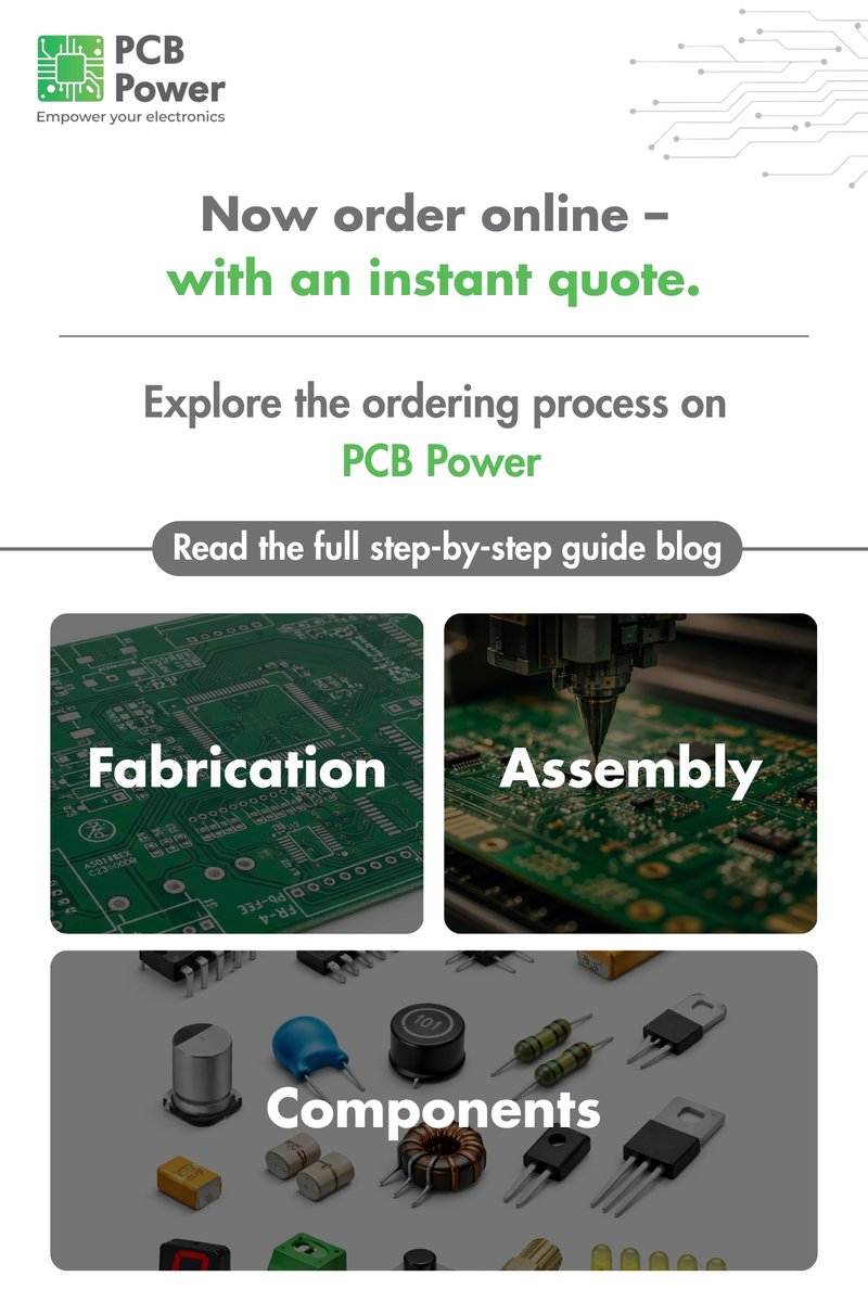
PCB fabrication, assembly, and component sourcing, all ordered online in one flow.
No back-and-forth. No manual tracking.
Read how it works: https://t.co/fkmUMN0snw
Some PCB failures don’t show up in inspection.
CAF forms inside the board long before field failure. Design decisions matter.
Read the CAF prevention guide - https://t.co/wlbSZxxczV
Before copper plating begins, PCB hole walls must first be made conductive.
Two established processes make this possible: electroless copper and direct metallization.
Learn more in our latest blog. - https://t.co/71Ru0k1mHw
#PCBFabrication#PCBManufacturing
Component placement decisions made early in PCB layout often decide how smoothly a design moves into assembly.
From board-edge clearance to spacing and thermal awareness.
Read the full blog:https://t.co/RMkUz7lGd4