🚀 MOSFET Logic Gates – Part 3: NOR Gate, Series Recap & DFM Best Practices
We’re wrapping up our MOSFET logic gate series with the NOR gate, a quick recap of all five gates, and practical DFM (Design for Manufacturability) tips.
🔹 NOR Gate Basics
Inputs → Output: 2+ inputs → 1 output
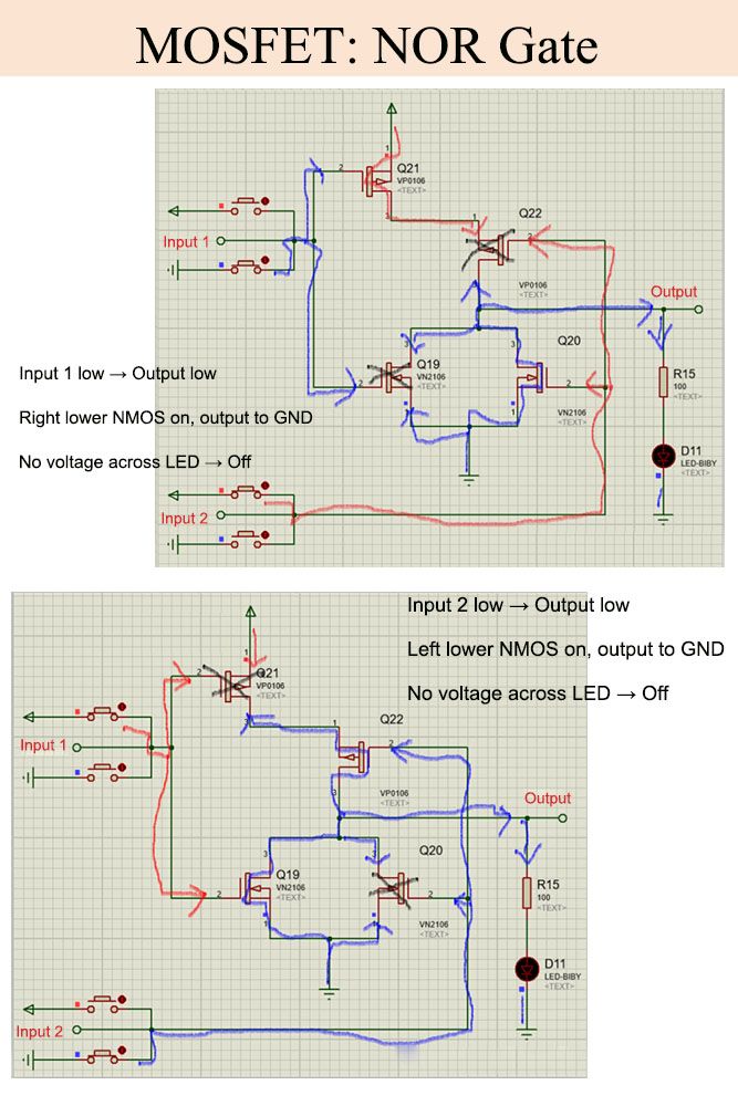
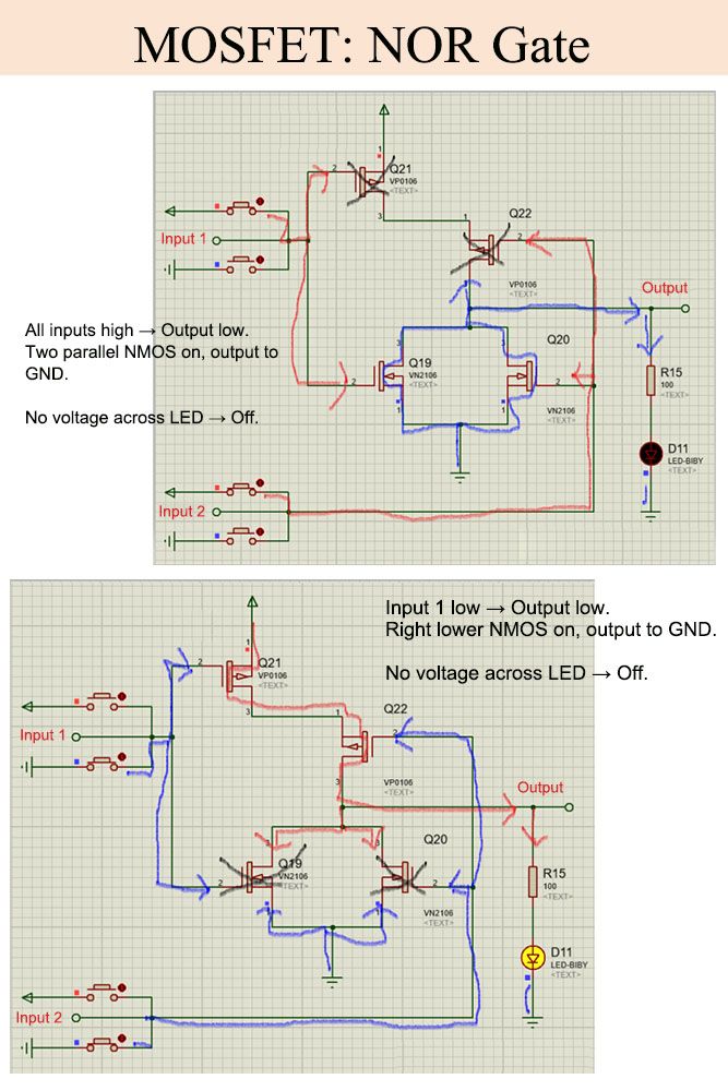
Logic: Output LOW if any input is HIGH; output HIGH only when all inputs are LOW.
🔹 How It Works (CMOS)
✅ All inputs HIGH → PMOS off, NMOS on → output LOW → LED off
✅ All inputs LOW → PMOS on, NMOS off → output HIGH → LED on
✅ Any single input HIGH → corresponding NMOS conducts → output LOW → LED off
💡 Tip: The NOR gate acts like a strict watchdog – one HIGH input instantly pulls the output LOW.
🔧 DFM Tips for MOSFET Logic Gates
🧵 Keep gate traces short and direct to minimize parasitic capacitance
⚡ Place decoupling capacitors close to VDD for stable power
🌡️ Use thermal relief on high-current MOSFET pads to avoid soldering defects
🔄 Maintain consistent MOSFET orientation & correct footprints to prevent assembly errors
📏 Ensure proper PMOS/NMOS spacing to avoid latch-up and ensure reliable switching
This concludes our series – blending functional logic with real-world manufacturability considerations.
Got a go-to DFM rule for MOSFET circuits? Drop it in the comments 👇
#MOSFET #LogicGate #NORGate #CMOS #ElectronicsEducation #PCBDesign #SMT #EmbeddedSystems #DFM
#PCBSync #PCBDesign #Electronics
GPT5.6sol Vs to GPT6 Astra PCB Layout —what exactly has been improved in PCB Layout? Model capability is the foundation, but engineering controllability is the key to mass production and deployment. In the next episode, we will continue to analyze what technical problems still exist in the engineering of the GPT-6 Astra version. Stay tuned for more~ #PCBSync #hardware #AIhardware #GPT6 #PCB #hardware #AI #engineering #layout #engineering #artificialintelligence #EDA #circuitboard #electronicinformation
Ever built a metal detector around a simple LC oscillator? 🌀
#PCBSync#PCBassembly#pcbmanufacturer#pcbdesign#pcb#pcba#circuitboard#electronics
These oscillators use a large-diameter exposed coil—its inductance changes in the presence of metal 🧲. The metal absorbs magnetic flux, creating a small frequency shift (up or down, depending on the material) 📡.
This particular circuit is the best performer I've tried:
Current draw: only 2 mA
Operating frequency: ~1 MHz
Listening in: just tune an AM radio to 1000 kHz — the beat frequency is easy to find on the dial.
No scope needed. Simple, low‑power, and reliable. Perfect for learning or quick metal‑sensing experiments.
#Electronics #Oscillator #MetalDetection #DIY #Engineering
Why does an LED need a resistor—and does it matter which side it goes on? An LED does not regulate its own current. In a simple voltage-powered circuit, a series resistor helps set the operating current. Example: with a 3.3 V supply, an LED forward voltage of approximately 2.0 V and a 330-ohm resistor, the current is roughly 4 mA. Actual forward voltage varies with the LED and its operating conditions. Put the resistor before or after the LED in the same series loop: it limits the same current. What would you change if you wanted to power two LEDs? Follow PCBSync for practical electronics, explained visually. #Electronics #CircuitDesign #LED #DIYElectronics #PCBSync
MOSFET Logic Gates – Part 2: NAND & OR ⚡
Continuing our deep dive into discrete MOSFET logic, this post breaks down the NAND and OR gates—covering how they operate, where current flows, and how to verify logic states with LEDs.
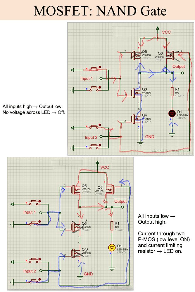
1️⃣ NAND Gate (NOT AND)
🔹 Inputs: 2+ → Output: 1
🔹 Logic:
All inputs HIGH → Output LOW
Any input LOW → Output HIGH
🔹 How it works:
All HIGH → N‑MOS network conducts → Output LOW → LED off
Input 1 LOW → Left P‑MOS conducts → Output HIGH → LED on
Input 2 LOW → Right P‑MOS conducts → Output HIGH → LED on
💡 Key insight: Any LOW input turns on the corresponding P‑MOS, pulling the output HIGH.
🎯 Takeaway: Opposite of AND — PMOS pulls up, NMOS pulls down.
2️⃣ OR Gate
🔹 Inputs: 2+ → Output: 1
🔹 Logic:
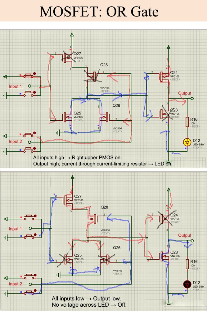
Any input HIGH → Output HIGH
All inputs LOW → Output LOW
🔹 How it works:
Any HIGH input → corresponding P‑MOS conducts → Output HIGH → LED on
All LOW → N‑MOS conducts → Output LOW → LED off
💡 Key insight: Each P‑MOS acts independently to pull the output HIGH.
🎯 Takeaway: A “diligent” gate – reacts as soon as any input is HIGH.
📐 CMOS principle: PMOS for HIGH, NMOS for LOW.
📌 Design-for-Manufacturing (DFM) Tips
Keep differential pair spacing consistent
Minimize parasitic resistance on PMOS pull‑ups (critical for OR/NAND speed)
Arrange layout for easy LED probing and visual debugging
🤔 Your turn:
In mixed‑signal PCB designs, do you prefer testing logic gates with LEDs first (visual, quick sanity) or oscilloscope signals (precise, timing‑aware)?
Let me know your go‑to method in the comments! 👇
#MOSFET #LogicGates #PCBLayout #CMOS #EmbeddedSystems #ElectronicsEngineering
#PCBSync #PCBDesign #Electronics
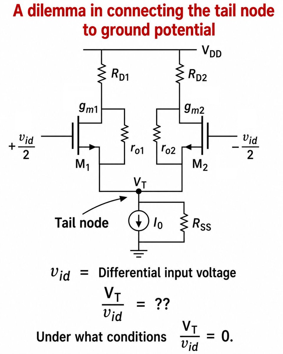
Analog Circuit Design Interview Question 💡
#PCBSync#PCBassembly#pcbmanufacturer#pcbdesign#pcb#pcba#circuitboard#electronics
Have you ever been unsure about when you can connect the tail node of an asymmetric differential amplifier to ground?
In a differential pair with a differential input, shorting the tail node to ground greatly simplifies analysis. But this isn't always valid. The real question is: Under what conditions can the tail node be treated as ground potential?
A good starting point is to evaluate VT / Vid and find the conditions that drive this ratio to zero.
What do you think? Share your insights below! 👇
#AnalogCircuits #CircuitDesign #InterviewPrep #DifferentialAmplifier #Engineering
MOSFET Logic Gates – Part 1: NOT & AND ⚡
We’re kicking off a series on MOSFET‑based logic gates, covering the five fundamentals:
🔹 NOT
🔹 AND
🔹 NAND
🔹 OR
🔹 NOR
Part 1 focuses on the building blocks – the NOT (Inverter) and AND gates.
We’ll look at MOSFET operation, visualize current flow with LEDs, and summarize key logic behavior.
1️⃣ NOT Gate (Inverter)
📌 1 input → 1 output
Logic:
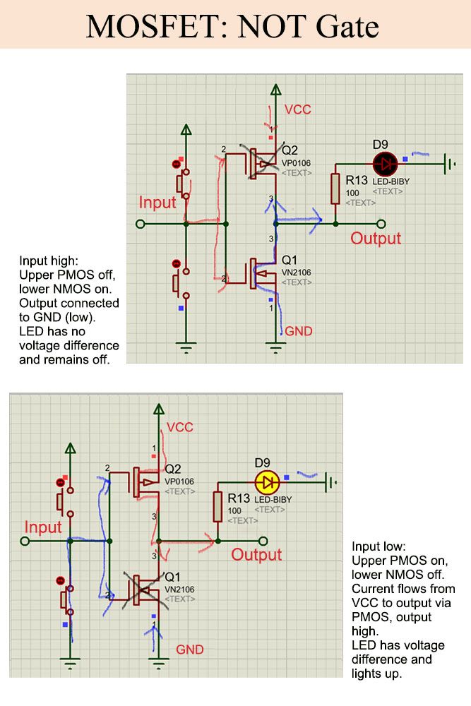
▪ Input HIGH → Output LOW
▪ Input LOW → Output HIGH
MOSFET operation:
▪ Input HIGH → Upper PMOS off, lower NMOS on → Output pulled to GND → LED off
▪ Input LOW → Upper PMOS on, lower NMOS off → Output pulled HIGH → LED lights
💡 Tip: Trace the current – only the active MOSFET conducts, creating the correct voltage across the load.
Key takeaways:
Simple inverter – output flips the input
PMOS pulls HIGH, NMOS pulls LOW
2️⃣ AND Gate
📌 2+ inputs → 1 output
Logic:
▪ Output HIGH only if all inputs HIGH
▪ Any input LOW → Output LOW
MOSFET operation:
▪ All HIGH → NMOS network conducts → Output HIGH → LED lights
▪ Any input LOW → NMOS network incomplete → Output LOW → LED off
💡 Tip: Think of the NMOS network as a chain – breaking any link breaks the output.
Key takeaways:
Requires all inputs HIGH to activate
MOSFET principle: PMOS pull‑up, NMOS pull‑down
📌 DFM Tips for PCB Layout
Keep NMOS pull‑down paths short and wide
Use series resistors with LEDs to prevent overcurrent
Avoid unnecessary crosstalk between inputs
❓ Which of these two gates do you find easier to implement on a PCB?
Drop your thoughts in the comments 👇
#MOSFET #LogicGate #NOT #AND #CMOS #PCBDesign #SMT
#PCBSync #PCBDesign #Electronics
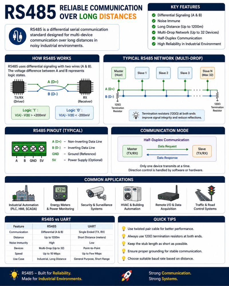
🚀 In modern automation, communication isn't just about sending data — it's about sending it accurately, consistently, and over long distances.
#PCBSync#PCBassembly#pcbmanufacturer#pcbdesign#pcb#pcba#circuitboard#electronics
That’s why RS485 remains a go-to standard in industrial communication. 🔌
Unlike basic serial protocols, RS485 uses differential signaling (A(+) and B(-) lines), transmitting data based on the voltage difference between the two lines. This design delivers outstanding immunity to electrical noise and signal interference.
✅ Key benefits:
Communication distance up to 1200 meters
Supports multiple devices on the same bus
High resistance to electromagnetic noise
Reliable operation in harsh industrial environments
Ideal for half‑duplex and multi‑drop networks
🔧 Common applications:
PLC & SCADA systems
Energy meters
HVAC controllers
Industrial automation panels
Remote monitoring systems
Building management systems
💡 Speed is impressive.
💡 Reliability is powerful.
In environments where failure is not an option, communication must be strong, stable, and dependable — and RS485 continues to deliver exactly that.
#EmbeddedSystems #RS485 #IndustrialAutomation #PLC #SCADA #Automation #Electronics #CommunicationProtocol #Engineering
One BJT, Three Amplifiers: Which Terminal Is Common?
Your sensor output looks fine on the scope. Connect the next stage and the voltage drops. Before adding gain, check whether the load is pulling the signal down.
The three BJT amplifier configurations solve different problems:
Common emitter (CE): Base in, collector out. Use it for voltage gain when an inverted output is acceptable.
Common base (CB): Emitter in, collector out. The output voltage stays in phase. Check that your source can drive the low input impedance.
Common collector (CC): Base in, emitter out. The emitter follower has voltage gain close to 1 and is useful as a buffer when the next stage would otherwise load the source.
The shortcut: “Common” tells you which terminal the input and output share as their AC reference.
If your sensor voltage sags when you connect the next stage, what would you measure first to confirm a loading problem?
#PCBSYNC #BJT #AnalogDesign #AmplifierDesign #ElectronicsEngineering #CircuitDesign
MOSFET ringing – when the clean PWM signal you designed isn’t what you get on the board.
In theory, your PWM waveform looks perfect.
In reality – once it reaches the MOSFET gate – small oscillations often appear after the rising or falling edge. That’s ringing.
🔴 It’s not just a waveform glitch
It’s easy to ignore ringing as a minor scope artifact. But if the peaks get too high, you can face:
Gate overstress
Unpredictable switching
Higher losses and heating
Worse EMI performance
This isn’t about aesthetics – it’s about reliability.
🔴 Common root cause: parasitic L & C
Ringing usually comes from the combination of:
MOSFET capacitance
Parasitic inductance in the gate-drive loop
Fast voltage/current transitions
Even a clean PWM source can produce ringing at the board level.
🔴 The PCB is often the culprit
A gate-drive loop that’s physically too large = more parasitic inductance.
Long traces, loose return paths, excessive driver–MOSFET spacing → ringing.
This is a layout problem, not just a MOSFET problem.
🔴 Start with physical fixes
Before adding exotic solutions, try:
Place the driver as close as possible to the MOSFET
Minimize gate loop area
Shorten traces and optimize return paths
Add or adjust a gate resistor to dampen oscillations
A small gate resistor often helps – but don’t overdo it. Too much resistance slows switching and increases loss.
🔴 Protection ≠ root-cause fix
Yes, a TVS or clamp can limit voltage spikes. But that’s protection, not a solution to poor layout or drive-loop design. Fix the cause, not just the symptom.
💡 Key takeaway
A perfect PWM signal at the controller doesn’t guarantee a clean waveform at the MOSFET.
What looks like a square wave on the schematic can behave very differently on the board.
Treat ringing as both an electrical and a physical design problem.
#PCB #MOSFET #PowerDesign #HardwareEngineering #ElectronicsEngineering #CircuitDesign #PCBDesign #EMC
#PCBSync #PCBDesign #Electronics
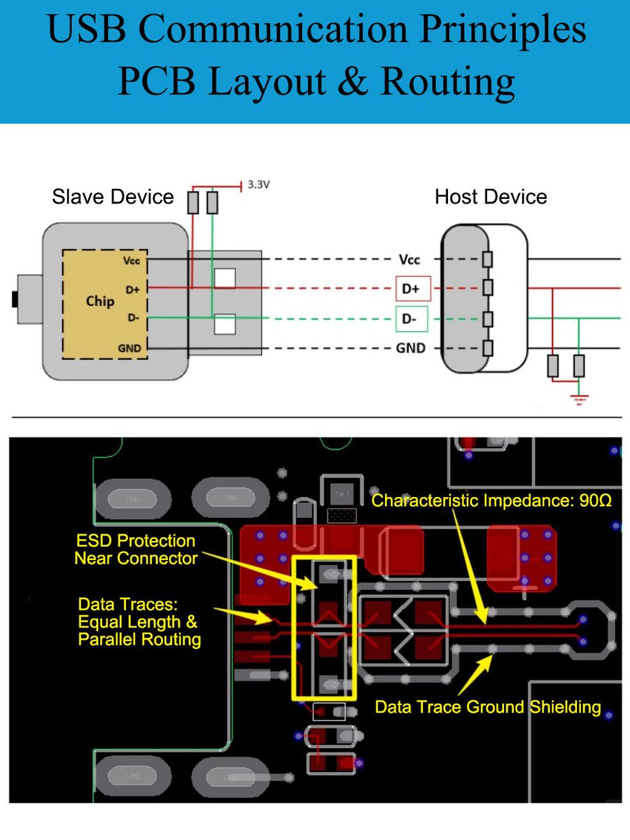
USB Communication Basics: PCB Layout & Routing Notes That Actually Matter 💡
#PCBSync #PCBassembly #pcbmanufacturer #pcbdesign #pcb #pcba #circuitboard #electronics
USB is everywhere in embedded design.
But in practice, most USB issues aren't protocol problems — they're layout and routing problems.
Here's a quick refresher on USB basics + the PCB rules that separate working prototypes from field failures.
🔹 USB communication in simple terms
USB handles both data and power over the same cable.
Host (PC, hub) initiates all communication
Device (MCU, peripheral) responds
Data travels over a differential pair (D+/D−)
Common versions to know:
→ USB 2.0: 480 Mbps, still the workhorse
→ USB 3.x: higher speed, extra pairs
→ USB Type‑C: reversible, now mainstream
🔹 Key PCB layout guidelines
1️⃣ Component placement first
USB connector close to board edge
MCU close to connector → short data traces
ESD protection as close to connector as possible (limits ESD current from entering the PCB)
2️⃣ Routing rules for D+/D−
Route as a matched differential pair
Keep equal length, parallel, constant spacing
Target 90Ω differential impedance
Avoid sharp corners, stubs, and unnecessary detours
3️⃣ Ground reference & shielding
Solid ground plane under the USB pair
Add ground shielding if routed on outer layers
Never split the ground under USB signals — a clean return path is critical
4️⃣ Via usage
Minimize vias on D+/D− (each via adds impedance discontinuity)
If vias are unavoidable, keep them symmetric on both lines
🔹 Common mistakes that kill USB
❌ Routing USB next to switching power traces
❌ Long, winding D+/D− routes
❌ ESD protection placed far from connector
❌ Broken or noisy ground under the USB pair
Result: enumeration failures, unstable connections, or EMC headaches.
🔹 A DFM reality check
Poor impedance control → board‑to‑board variation
Excessive vias → lower yield at higher speeds
Clear stack‑up definition is required for consistent 90Ω differential impedance
"Good design is buildable design."
What's the strangest USB layout issue you've debugged? 👇
#PCBDesign #USB #HighSpeedDesign #SignalIntegrity #HardwareDesign #DFM