After speaking with several engineers across the optical industry, I noticed something interesting.
As CPO moves toward mass production, there's one component they consistently believe deserves much more attention.
Engineers from different companies kept bringing up the same thing.
Any guesses what it is?
This might be the most important announcement from $NVDA this week.
NVIDIA plans to expand CPO optical engine manufacturing capacity by 15x by mid-2027 and potentially 30x by the end of 2028.
Meanwhile, $AMKR targets over 300% growth in advanced packaging capacity, and NVIDIA is advancing $1.1B to KYEC for testing infrastructure.
CPO is moving beyond technology validation into large-scale manufacturing infrastructure.
I'm not just watching lasers. I'm watching optical assembly, wafer-level testing, known-good die, and interposers.
The market may not have discovered all the real winners of the optical revolution yet.
Did you see what $NVDA just announced?
While Wall Street debates the AI bubble, NVIDIA is aggressively expanding its supply chain.
- Substrate capacity: 2.5x over 3 years
- Advanced packaging: 4x+ by end of 2028
- CPO optical engine capacity: 15x by mid-2027
That last number deserves serious attention.
The market is questioning AI demand. NVIDIA is preparing to manufacture the next generation of optical interconnects at scale.
$NVDA $COHR $LITE $AVGO
The central theme is cost per good chip: the article connects ASML parts pricing, High-NA lithography, and advanced bonding through productivity, yield, and manufacturing economics.
Shorter HBM stacks do not necessarily mean less packaging investment: TrendForce reportedly sees some customers considering 8-high instead of 12-high, potentially increasing base-die and per-stack testing demand for a fixed DRAM supply.
Optical testing must distinguish product defects from measurement error: FormFactor’s alignment and calibration technologies address false failures, while volume production also requires sufficient test throughput.
Nutty’s Research connects ten equipment developments to the manufacturing problems they address. Its distinction between GF’s interposer manufacturing and Amkor’s assembly and testing helps clarify each company’s role.
The connection to optical testing is clear: stable measurements are necessary to understand yield and improve manufacturing. Production adoption, repeat orders, and shorter test times will show how that need translates into equipment business.
Stocks have fallen so much.
I want to buy, but I can’t decide what.
On the way up, everything looked promising. On the way down, every concern sounds convincing.
Guess this is when I need to do my homework.
- Jensen Huang claims $NVDA AI chips carry the lowest risk of any asset due to high residual value and versatility across workloads.
- He suggests AI accelerators could serve as collateral for loans, arguing financiers underestimate their long-term flexibility.
- H100 and B200 chips have retained or appreciated in value; B200 reportedly trades at 158% of original purchase price in secondary markets.
> Huang's collateral argument reflects growing confidence in AI accelerator durability and secondary-market liquidity, which could lower financing costs for hyperscaler capex and support sustained $NVDA hardware demand even as new chips release.
> However, residual value depends on workload compatibility and system configuration, limiting blanket applicability as collateral.
The most valuable insight from Damnang's latest expert call is not simply ASML's dominance in EUV lithography, but the economic limits of that dominance.
The interview connects High NA adoption, manufacturing lead times, supplier bargaining power, and fab economics into one framework.
It also examines Terafab and China's domestic EUV ambitions.
The AI scale-up optics race is getting more interesting.
ams OSRAM just showcased its 850nm top-side VCSEL architecture with dense electrical I/O.
- 25µm-pitch microVCSEL arrays
- 3D integration using silicon TSVs
- Demonstrated 32Gb/s at ~0.25pJ/bit
The real story isn't just faster optics. It's packing massive numbers of low-power optical channels into a tiny footprint.
If you're only watching CPO, you might be missing half the AI optics opportunity.
Today I had in-depth conversations with optical, packaging, and system design engineers at Intel, NVIDIA, Marvell, Micron, Broadcom, and Ayar Labs.
My takeaway is that optics is just getting started. Don’t put a ceiling on how big it can get.
Investing is still hard. Conversations like these strengthen my conviction to keep going.
- Gemtek and Starman partner to establish U.S.-based optical transceiver manufacturing
- Domestic production capacity reduces supply chain dependency for the market
> The partnership signals effort to nearshore optical transceiver production, likely responding to supply chain resilience concerns and potential tariff considerations.
> This could reshape regional manufacturing dynamics and create new sourcing options for customers.
- $INTC begins tool installation at Fab 62 in Arizona, marking transition from construction to equipment deployment for 2028 operational target.
- High-NA EUV scanners costing $350-380 million each are being integrated; $INTC expects Fab 62 to support 14A node high-volume manufacturing in 2028.
- Tool installation signals capital commitment and real operational timeline rather than aspirational plans for the facility.
> $INTC's tool installation at Fab 62 signals concrete capital deployment for advanced node manufacturing; successful High-NA EUV ramp at 18A (operational since October 2025) validates the technology readiness for 14A in 2028, positioning $INTC to compete on leading-edge node capacity against $TSM and Samsung.
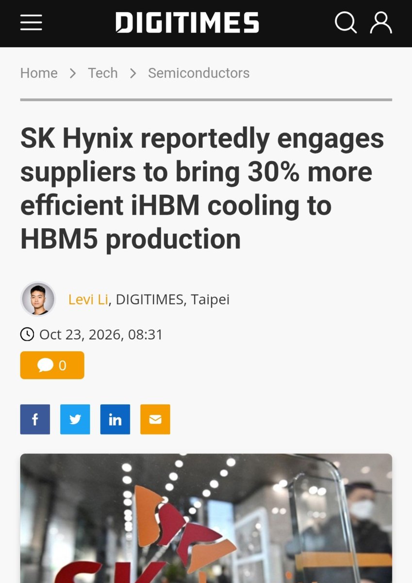
- SK Hynix is engaging suppliers to improve cooling efficiency for HBM5 production
- Reported 30% efficiency gain in iHBM cooling suggests cost and thermal management advancement
> SK Hynix is working to enhance thermal efficiency in HBM5 production, which could reduce manufacturing costs and improve product reliability for next-generation AI chips.
> This operational improvement suggests the company is positioning itself competitively as HBM demand scales.