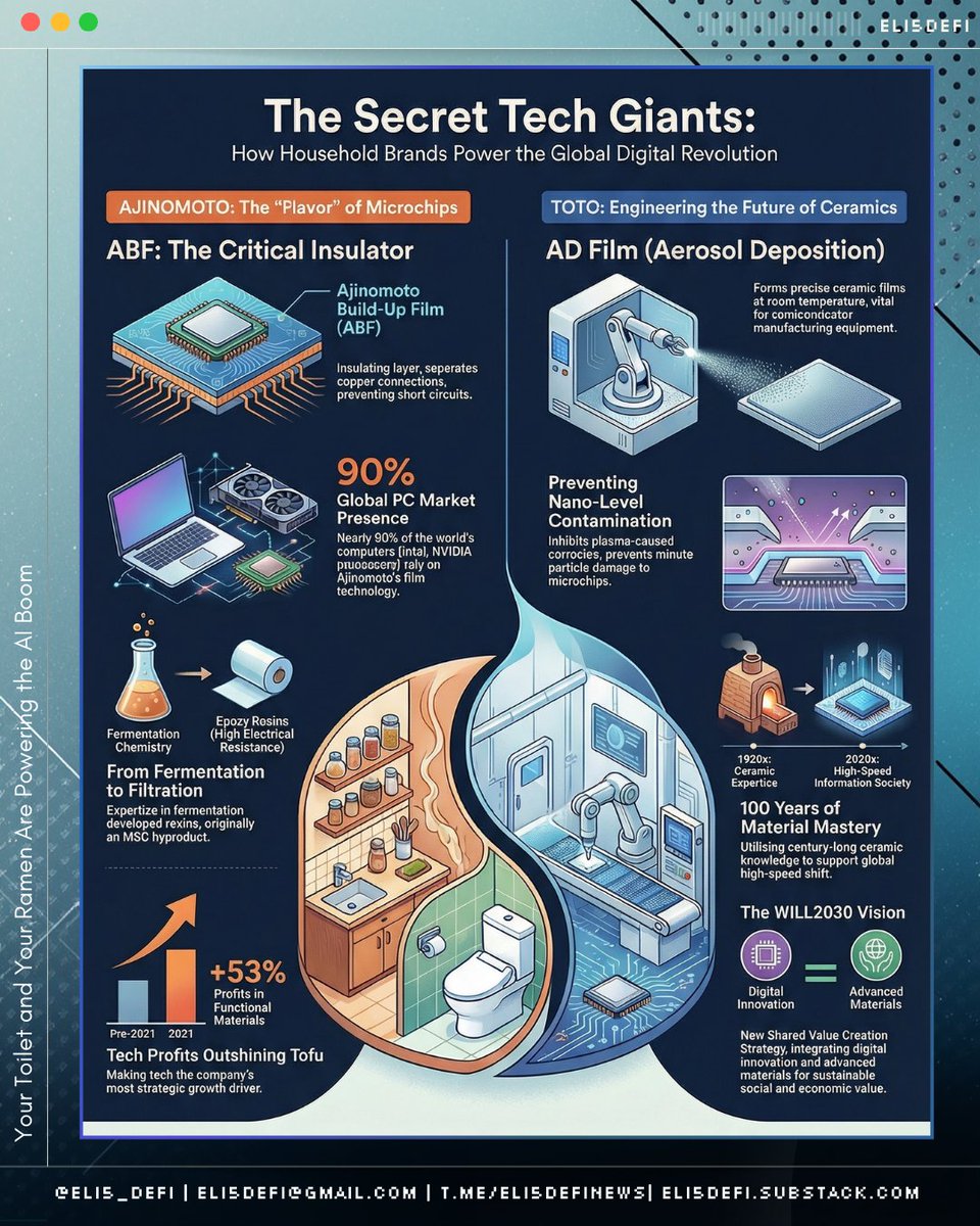
Your Toilet and Your Ramen Are Powering the AI Boom
The company that makes your MSG also makes the critical material inside every single NVIDIA chip.
I wish this were a metaphor. It’s not.
This is the actual, unglamorous semiconductor supply chain that everyone is overlooking while throwing billions at software startups.
Let's talk about it.
—
➠ Ajinomoto: Sprinkling Umami on the Tech Sector
Ajinomoto owns roughly 98% of the insulating foundation inside every high-performance AI chip.
Inside chip packaging, there is a micrometer-thin insulating layer called Ajinomoto Build-up Film (ABF) that separates copper traces. Without it, your $40,000 chip essentially short-circuits or melts into an expensive puddle under thermal stress.
Intel uses it. NVIDIA uses it. AMD uses it.
How did this happen?
Back in the 1970s, Ajinomoto researchers were staring at a chlorinated byproduct from their MSG production and thought, "What if we mixed this with epoxy resins?"
The result was a freak of chemistry: it had massive electrical resistance and exceptional heat tolerance. By 1999, it was commercialized as ABF. An accidental polymer from a seasoning factory is now the literal foundation of modern AI.
The moat is basically impenetrable. Tech giants have funded competitors to try and break the monopoly, but it turns out that decades of soup-factory polymer science is hard to replicate.
Qualification cycles take up to two years, and even then, you're just trying to match a standard Ajinomoto perfected when we were still using dial-up internet.
—
➠ Toto: From High-Tech Bidets to High-Tech Chips
Toto makes toilets. Toto also makes the ceramic platforms that hold silicon wafers during AI chip etching.
During semiconductor fabrication, silicon wafers have to be held perfectly still while being blasted with high-heat plasma. The tool for this is an "electrostatic chuck," which clamps the wafer using electric fields in a vacuum at extreme temperatures.
Enter Toto. Yes, that Toto.
They manufacture these chucks using fine ceramics, the exact same material science behind their world-class bathroom products.
Their proprietary Aerosol Deposition (AD) process applies a dense yttria (Y₂O₃) film that flexes on metal components in two ways:
It survives plasma erosion: So the multi-million-dollar tools last longer.
It reduces particle contamination: When you are printing circuits at nanoscopic scales, one stray speck of dust ruins the whole chip. Who better to keep things impeccably clean than the kings of the Japanese bidet?
Wall Street is finally catching onto the joke.
Activist investors and Goldman Sachs analysts have both flagged Toto as a massively undervalued AI infrastructure play. T
heir semiconductor ceramics segment made up roughly 42% of their operating income heading into 2025. The market is officially re-rating them from "consumer staple" to "AI infrastructure", they just had to look past the bathroom branding.
—
➠ Japan's Tech Strategy: Raid the Bathroom Cabinet
This is a full ecosystem story. Japan's "Great Material Pivot" basically sounds like a grocery run:
❶ Nippon Electric Glass:
Shipping samples of 510mm glass substrates by 2026. Because AI chips are getting so hot that plastic is failing, they're pivoting to high-tech glass.
❷ Sumitomo Bakelite:
Holds a 40% global market share in epoxy resin used to encapsulate chips, expanding their plants just to keep up with the AI gold rush.
❸ Kao Corporation:
The soap company! They are out here supplying specialized wafer cleaning agents to optimize chip yields. Because cleanliness is next to godliness, especially in semiconductors.
A century-old Japanese manufacturer solves a household annoyance, realizes the exact same chemistry works for quantum-level tech, and quietly becomes the backbone of global computing.
Casual.
The global semiconductor ceramic market is projected to hit 1.6 trillion yen by 2030. The drivers? Meta, Google, and Amazon aggressively building out data centers full of hardware resting comfortably on toilet ceramics.
—
➠ The Real Takeaway
The AI boom isn't just magic algorithms floating in the cloud; it has a very physical, very weird substrate.
Yes, not all about new LLMs model or Seedance New IP Abuse Video.
Every NVIDIA H100 churning out AI responses right now is sweating on a porcelain tile, wrapped in MSG.
That supply chain is highly concentrated, nearly impossible to replicate, and totally invisible to the people building apps on top of it.
This is the part of the AI trade that everyone misses when arguing about which frontier model will win. The "picks and shovels" of this gold rush aren't just TSMC and ASML, they are Osaka chemistry labs and ceramics factories that predate the microchip by decades.
So the next time an AI demo blows your mind, just remember: the only reason the whole thing doesn't explode is because of soup byproducts and a toilet manufacturer.
bikin tangga gagal mulu gagal mulu kocak.
mertua ikut campur terus akhirnya 2x kerja tetep salah
dan skrg tiap anak tangga tingginya mau beda2
PLISSS BANTUIN AKU TINGGI RUANGAN 4 METER INI GIMANA BIKIN TANGGANYA😭😭😭😭
I just can’t stop laughing baca cerita yg lagi viral di FB. Ibuk-Ibuk kehilangan suaminya di hutan, pamitnya pergi berburu. Ternyata nyasar nya di… ATLAS BEACH CLUB 😭😭😭