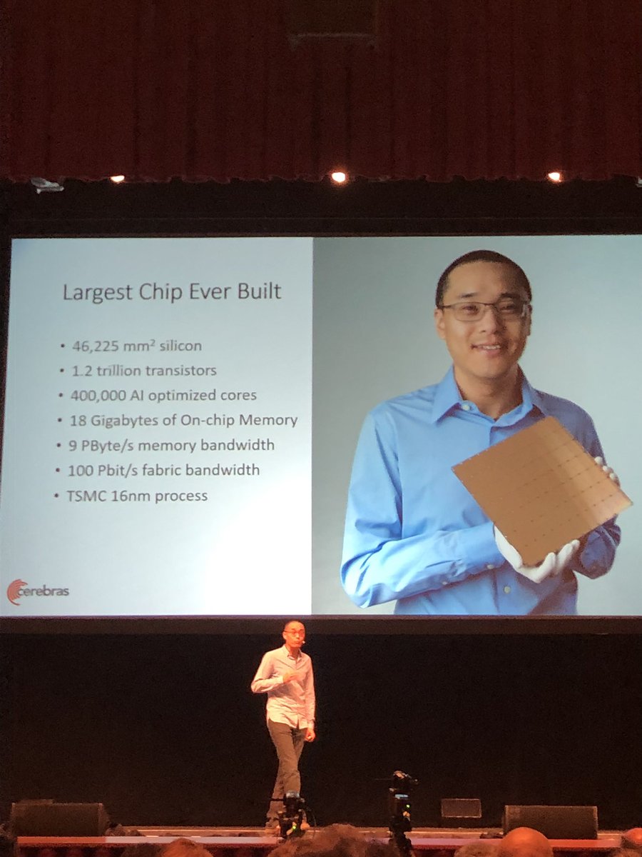
Ten years ago, we started @cerebras around an approach many believed was impossible.
As a computer architect, it is hard for me to imagine a more exciting time. Model releases are accelerating, and hardware tapeout is compressing from multi-year roadmaps to annual launches.
Hot Chips is my favorite conference, and it’s where I launched Cerebras 7 years ago. This year’s conference was especially exciting, and so much innovation was shared. I am watching the industry recreate itself: SRAM is mainstream, DRAM is moving into the third dimension, networks are being fundamentally redesigned, and AI is helping design and program the chips themselves.
The industry has never moved faster and some of the hardest architectural questions are still wide open.
It was also good to see the range of approaches to stacked DRAM at Hot Chips. This is also a problem we’ve been working on for a while. The common challenge is balancing bandwidth, capacity, thermals, yield, and manufacturability as AI memory demands keep rising.
With DMatrix, I was excited to see the industry pushing to 3D stacked DRAM with promising design directions.
Current DRAM memory bandwidth is limited by the interface between the DRAM chip and compute chip. The length of the linear edge (aka, beachfront) between the chips limits the number of bits that can cross between the DRAM and compute chips. With HBM DRAM, the memory bandwidth is limited to order ~10 TB/s to compute chip, or order ~10 GB/s/mm2 of compute silicon.
By stacking the DRAM chip on the compute chip with 3D integration, you can potentially increase the interface to use the entire area of the chip and therefore increase the bandwidth. DMatrix projects order ~30 GB/s/mm2 of compute silicon which is ~3x higher bandwidth than traditional HBM.
The concept has been around for a long time but it is not easy. There are fundamental integration challenges in the bonding technique, power delivery, thermal management, packaging, testability, yield, and reliability.
On the performance front, at 3x higher bandwidth than traditional HBM DRAM, the gap between 3D DRAM and SRAM architectures is still wide. As an industry, reducing that performance gap is fundamental to capturing the full potential of stacked DRAM.
Memory bandwidth is the main bottleneck limiting inference decode speed so finding new ways to increase memory bandwidth is imperative to move our field forward. This is why I am excited to see when the promise of 3D stacked DRAM can be realized by solving these fundamental challenges.
With Jalapeño, OpenAI designed a better GPU. And it is very impressive that in such a short timeline, the Jalapeño team brought it from concept to running performance workloads in the lab.
The future is clearly AI driven chip design and programming kernels. Jalapeño's push for higher speed and faster inference is absolutely right. It’s encouraging to see validation of the need for speed. Bringing faster inference across the spectrum will lift the tide for the entire industry.
By removing many of the overheads in a traditional GPU design, Jalapeño has pushed what’s possible for an optimized DRAM-based architecture.
The difference with SRAM-based architectures is the following. DRAM uses a different silicon process vs. the process used for compute, whereas SRAM uses the same process as compute. The DRAM process enables it to have higher density and more capacity. Because it uses a different process, DRAM is a physically separate chip than the compute chip. Since SRAM uses the same process, SRAM is directly embedded into the compute chip.
Given that DRAM is a separate chip and SRAM is on-chip, DRAM is order ~50x lower bandwidth than SRAM (~10 TB/s HBM to compute chip vs. >100 TB/s SRAM on compute chip). And DRAM is order ~30x higher power per bit than SRAM (3 pj/bit DRAM vs. 0.1 pj/bit SRAM).
When you run a model, the memory bandwidth and power determine the decode speed because all of the active weights need to be read from memory, serially one token at a time. As a result, SRAM-based architectures have faster decode speed. DRAM-based designs have higher capacity.
I’m really excited to see a future when more optimized DRAM-based designs like Jalapeno are used alongside SRAM-based designs to get the best of both worlds.
It was also encouraging to see how SRAM-based architecture is entering the mainstream with LPX.
With 150TB/s of memory bandwidth, an LPX has ~15x more memory bandwidth than a single Rubin die. The higher memory bandwidth enabled them to show 3400 tps decode speed on Gemma 4 31B. That level of speed is not possible on a traditional HBM DRAM-based design and showcases the value of SRAM-based architectures on a popular small model.
With 500MB of SRAM per chip, scaling to larger modern models will require many more LPX chips. Consider a frontier-level model with trillions of parameters, such as Kimi K3 2.8T. Storing the 4b weights alone requires ~1.5TB, or ~3,000 LPX chips for a single model instance. That assumes 100% of the memory is available for weights and does not include the KV cache.
The KV cache could require another ~1.5 TB (e.g. 27KB per token × 300K sequence length × 200 concurrent requests). Now we are at 6,000 chips, again assuming 100% memory utilization. When factoring for other memory overheads, the number is likely 10,000 chips or more - to run one instance of a large frontier model.
Connecting thousands of chips at high bandwidth and low latency is not easy and has overheads in performance, power, cost, and reliability.
If they do Attention-FFN disaggregation in the future, they could theoretically reduce the number of LPX chips needed by keeping the KV cache off the LPX chips that run only the FFN. However, the weights alone would still require thousands of chips. Attention-FFN disaggregation is also complex because every token has to ping-pong between different hardware on every single layer of the model.
SRAM is essential for fast, low-latency inference, and it is encouraging to see the industry moving in this direction. But for SRAM-based architectures, speed is only part of the equation. To scale, you need enough of it.
The latest updates from Rubin at Hot Chips continued to demonstrate NVIDIA’s relentless improvements in throughput.
The Rubin architecture is incredibly efficient at highly parallel workloads where the arithmetic intensity is high. This is why it is such an efficient architecture for training where high batches are common.
In inference, the roofline is ~2200 FP4 FLOPs/byte (50 PFLOP/s / 22 TB/s). That means for every FP4 weight in DRAM, Rubin needs to reuse it for ~550 MAC operations to sustain high throughput. During inference, this occurs during 1) prompt processing or 2) high batch decode.
In prompt processing, since all of the tokens are known up front (i.e. the user or agent provided them), they can all be processed together making it easy to achieve at least ~550 parallel tokens reusing the same weights for high throughput.
In decode, even though the attention has higher arithmetic intensity, the overall model is limited by the experts and other projections resulting in only <5 FLOPs/byte for models like Deepseek V4 and Kimi K3 even at long 100k+ context. Therefore, high throughput is achieved by using large batch size, by processing multiple requests at the same time. Doing so enables reusing the weights across tokens from all of those requests to maintain high throughput. But running at high batch size reduces the decode speed, or interactivity, as seen in pareto curves.
For this reason, Rubin continues to set the throughput benchmark for low interactivity inference. And, with its high prompt throughput, and with the rise of disaggregated inference, it is also extremely well suited for prompt processing in heterogeneous disaggregated environments.