Powerchip Raises DRAM Foundry Prices Another 45% in July; Logic Process Capacity Hits 1.4× Booking Ratio as Mature Nodes Face Severe Shortages
Powerchip’s gross margin improved to 28% in the second quarter of 2026, and the company expects profitability to continue rising through the third and fourth quarters.
Chairman Frank Huang believes the upcycle is only beginning. Looking ahead to 2027, he expects gross margins across the wafer foundry industry to exceed 40%, not only for Powerchip but also for its major peers and competitors, including UMC and Vanguard International Semiconductor (VIS). According to Huang, the industry’s outlook remains exceptionally strong, supported by robust demand and tightening capacity across mature process technologies.
https://t.co/Ydyiz3Zxgj
Lenovo, the world’s biggest PC vendor, is now shipping laptops to the US equipped with storage drives (Solid State Drives) from Yangtze Memory Technology (YMTC), media report, marking the entry of China-brand memory to the global PC market. https://t.co/HQhQWDh1dz
AP시스템, 반도체 장비 2030년 매출 비중 30% 목표
1/ AP시스템이 반도체 장비 사업 비중을 확대한다. 현재 10% 내외인 매출 비중을 2030년까지 30% 수준으로 늘릴 계획이다. 디스플레이 장비에서 쌓은 레이저와 열처리 공정을 반도체 사업으로 확장하는 것이 핵심이다.
2/ AP시스템은 급속 열처리 장치(RTP)를 포함한 반도체 장비 R&D 프로젝트를 10개 이상 진행 중이다. 반도체 장비 전담 인력도 2024년 말 6070명에서 현재 160170명으로 크게 늘렸다.
3/ 반도체 장비 매출 중심은 RTP 장비다. 이 장비는 웨이퍼를 단시간 고온 처리한 뒤 급속 냉각해 표면을 평탄화하고 손상을 완화한다. 2022년부터 RTP 장비로 600억원 규모 매출을 기록했으며 현재 D램 3개, 낸드 2개 공정에 공급 중이다.
4/ 분석용 레이저 다이싱 자동화와 레이저 디본더도 개발한다. 레이저 디본더는 OLED 기술을 반도체 글래스 캐리어 분리 장비로 전환하는 것으로 고객사 평가 단계에 있다.
5/ AP시스템의 사업 기반은 디스플레이 장비지만 최근 중국 업체 투자로 가격 경쟁이 심화했다. 반도체 장비 확대는 매출 구조 다변화 조치다. 올해 1분기 매출 비중은 디스플레이 88%, 반도체 11%다.
Intel’s EMIB-T is trying to attack TSMC where TSMC is most constrained: advanced packaging (not leading edge wafers)
imo the best way to tell EMIB-T is working is if Google TPU v9 ships in volume, on schedule, with HBM4-class memory, acceptable yields + Intel/partner revenue visibly ramps.
CXMT의 EUV 없는 '본딩 D램'은 결코 싼 방법은 아니다. 그러나 위협적인것은 사실
1. 본딩 D램은 셀 어레이와 페리 회로를 각각 다른 웨이퍼에 만들고 붙이는 기술임.
셀 웨이퍼는 DUV 멀티패터닝만으로 높은 셀 밀도를 뽑을 수 있어서 EUV 규제를 우회하는 카드가 됨.
한경 보도 기준 CXMT는 허페이에 R&D 라인을 짓고 파일럿 테스트 중이고, 삼성전자도 B1b 프로젝트로 유사 기술 개발 중임.
2. 그런데 원가 구조를 뜯어보면 만만치 않음. 일단 웨이퍼가 2장, 셀 웨이퍼를 뒤집는 공정까지 감안하면 캐리어 웨이퍼 포함 3장이 들어감.
여기에 W2W 본딩은 불량 다이를 미리 골라낼 수가 없어서(No KGD) 셀 수율 x 페리 수율 x 본딩 수율이 곱셈으로 작동함.
각각 90%씩만 나와도 합산 73%.
즉, EUV를 안 쓴다고 원가가 싸지는 게 아님.
3. 셀 노드도 차이가 남. CXMT 현재 최선단이 G4(16나노급)라 본딩 D램 셀도 1a급 수준에서 시작할 것으로 추정됨.
메모리 3사는 1c 이후 선단 셀로 붙일 예정이라 셀 자체의 밀도 격차는 여전히 존재함.
4. 특허 자료 보면 접근 방식도 갈림. 삼전/하닉/마이크론은 Fusion Bonding 쪽인 듯함.
셀 웨이퍼를 서포트 웨이퍼에 붙여 뒤집는 방식이라 본딩 계면에 접점이 필요 없음.
반면 CXMT/YMTC는 바로 Hybrid Bonding으로 가는 그림. 완성된 셀 웨이퍼와 페리 웨이퍼를 전기적으로 직접 붙이는 건데, 이건 50nm 이하 피치 본딩이 필요해서 현재 최선단 대비 한 자릿수 아래 수준임.
3사가 안 하는 게 아니라 아직 못 가는 영역에 중국이 먼저 베팅한 셈.
5. 그래도 CXMT가 가는 이유는 명확함. 얘네한테 비교 대상은 'EUV D램'이 아니라 'D램을 못 만드는 것'임.
반도체 첨단장비 제재 하에서는 웨이퍼 3장 쓰는 게 유일한 선단 경로라 경제성 계산 자체가 다름.
보조금에 내수 수요까지 받쳐주고, IPO로 42억달러 조달해서 차세대 라인 확충할 계획이기도 함.
6. 낸드에서 이미 본 그림임. 2018년 YMTC가 Xtacking 들고나왔을 때 업계 반응이 "웨이퍼 2장? 저걸 왜 쓰나"이었음.
근데 기술이 누적되면서 하이브리드 본딩 핵심 특허가 YMTC 119건 vs 삼성 83건, 하이닉스 11건(23년 기준)이 됐고, 삼성이 차세대 낸드에 YMTC 특허를 라이선스했다는 보도까지 나옴. 조롱받던 기술이 특허 장벽이 된 것.
새로운 시도를 먼저 한다는 것 자체가 큰 자산임.
*개인적으로 걱정되는건 낸드에서 그랬듯 D램 본딩 세대에서도 특허 지형이 중국 쪽으로 기울어서 역전되는 상황이 걱정.
이외에도 Cell자체를 쌓는 3D DRAM에서도 무섭게 치고 오는중.
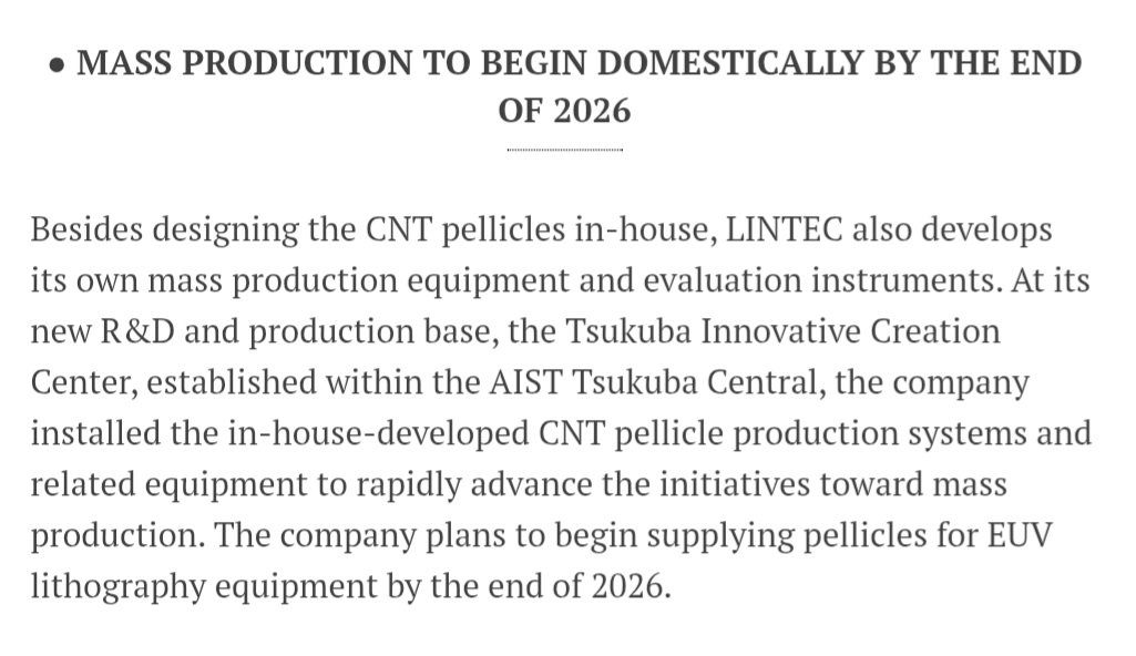
LINTEC will begin shipping its new carbon nanotube EUV pellicles to customers by the end of the year, as it enters the production ramp phase.
The company claims 90% transmittance and a 66x improvement in reliability (measured by exposures before failure). Game changer if this proves out.
In China, Huawei’s Tingbo He releasing the second revised edition of the Tau Scaling Law paper is a hot topic.
Some are praising it for bypassing EUV and significantly improving chip performance even without it.
Here's some paper's table
paper link: https://t.co/fEwDmYZN3z
인텔은 차세대 패키징 'EMIB-T' 이후의 조립 공정을 이미 특허로 출원했습니다. EMIB-T가 학술대회에 소개되기 15개월 전 입니다. 최근 보도된 EMIB-T 기술이 브릿지에 전력 비아(Power Vias)를 도입하는 데 집중했다면, 이 출원서의 핵심은 브릿지의 위치를 기판(보드)에서 칩으로 옮기는 데 있습니다.
현재 인텔의 방식은 기판 내부에 작은 브릿지 다이를 묻고 그 위에 칩을 실장합니다. 반면 출원된 새 공정은 브릿지를 칩에 먼저 접합하여 '멀티 다이 어셈블리'를 구성합니다. 가장 큰 차이는 기판을 연결하기 전에 클러스터 전체를 먼저 시험한다는 점입니다. "성능 지표 통과 여부를 판단하기 위해 어셈블리를 테스트한다"는 청구항 명세서 내 설명처럼, 테스트를 통과한 조립체만 최종 기판과 결합시킵니다.
이는 패키징 수율을 고려한 공정 설계입니다. 다이 하나만 불량이어도 패키지 전체를 폐기해야 하므로, 고가의 기판을 결합하기 전에 결함이 있는 클러스터를 선제적으로 걸러내는 것입니다. 발명자 13인 중 EMIB 원천 특허의 주역인 라빈드라나트 마하잔(Ravindranath Mahajan) 님이 포함된 점은, 이 기술이 인텔 패키징의 핵심 조직에서 개발되었을 가능성이 높다는 것을 암시합니다.
다만 이 문서는 아직 심사 중인 공개 출원이며 확정된 등록 청구항은 아직 없습니다. 아래의 아티클에서, 저는 이 출원서가 차세대 패키징의 형태를 어디까지 구체화했는지, 그리고 현재 특허청 심사 과정에서 어느 단계에 있는지를 분석해 보았습니다. 😁
This is extremely interesting. If Intel’s strategic shift succeeds, it could overturn the balance of power against TSMC. But if it fails, it could lead to disastrous yields and customer defections, much like what Samsung Foundry went through in the past. It’s a remarkably bold gamble.
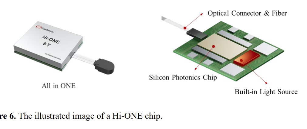
At ECTC 2025, Sumitomo Electric Industries, Ltd. presented a groundbreaking paper titled “Flip-Chip Photonic-Electronic Integration Platform for Co-Packaged Optics using a Glass Substrate with Vertically-Coupled Beam Expanding Lens.” This work introduces an innovative CPO (Co-Packaged Optics) integration platform that combines a glass substrate with 3D-printed Vertically-Coupled Beam Expanding Lenses (VCBELs)—offering a novel solution to the long-standing alignment and packaging challenges in photonic-electronic co-integration.
https://t.co/3zdKxsl0UE
Traditional geometric shrink was always about cutting RC delay anyway (smaller transistors + shorter wires = faster signals).
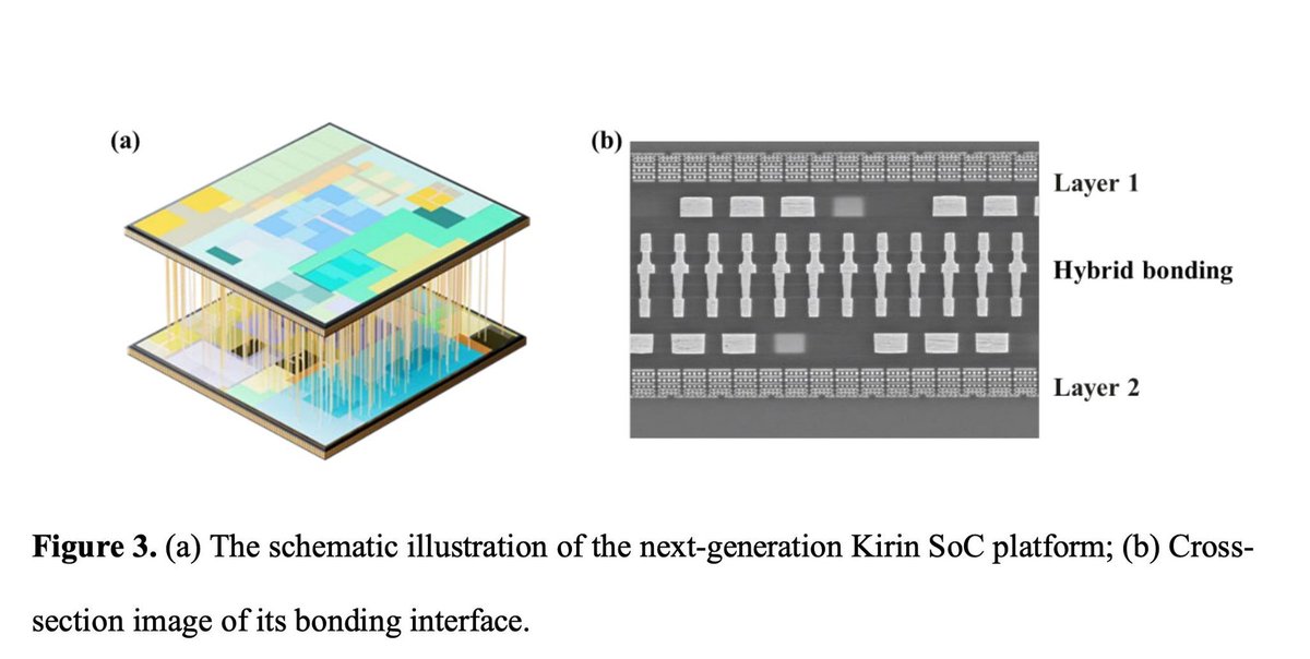
Now that shrinking is slowing, Huawei is folding critical logic paths across two wafers with super-dense 1.5μm hybrid bonding, basically treating the stack like one giant chip.
Result in the Kirin 2026?
41% better energy efficiency at same performance vs a planar baseline on the same node.
AMD/Intel 3D is cool, but their bonding pitches are still 6-9μm.
This feels like the next level.
I've been discussing Huawei's τ scaling (temporal scaling) with people recently, and noticed the conversation tends to stay at the surface level without reaching its substance — likely because many participants don't come from an EE background and aren't familiar with the classical meaning of τ in circuit theory. The very first time constant you learn in a circuits course is τ = RC: the resistance of a wire multiplied by its capacitance gives the order of magnitude of the time a signal needs to traverse that wire. The longer the wire, the greater the resistance and capacitance, and the slower the signal. Within this framework, the past sixty years of geometric scaling are reinterpreted as one particular implementation of temporal scaling. Transistors were shrunk to shorten switching delay; circuits were packed more tightly to shorten metal interconnects and reduce signal propagation delay. Geometric scaling was only ever the means — compressing delay was always the end. Huawei's thesis is that once geometric scaling stalls, you find other ways to keep compressing delay.
As it happens, He Tingbo's τ scaling paper released its v2 a couple of days ago, expanding from 16 to 23 pages. I compared the two versions: the data and conclusions are unchanged. The additions are essentially responses to several points of criticism the industry raised about v1. Three are worth discussing.
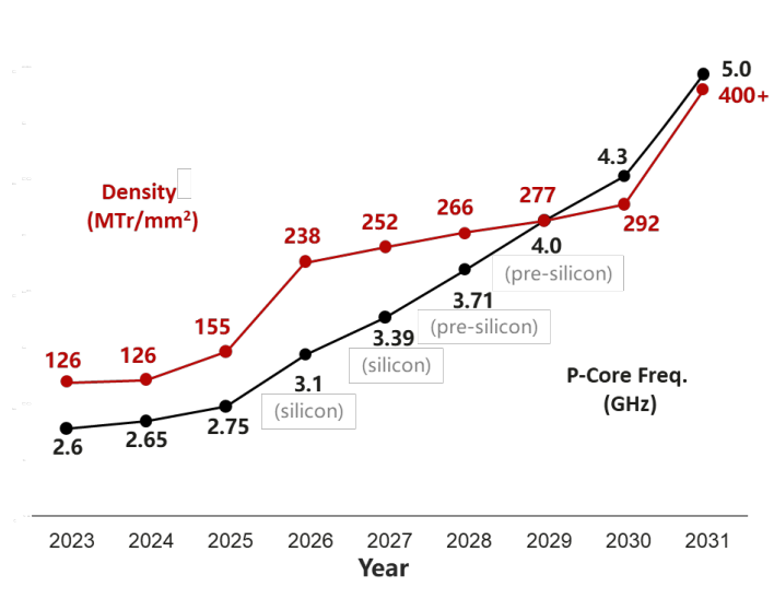
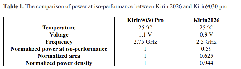
The most important addition is the test evidence now backing the previously bare claim of "41% energy efficiency improvement." In v1, that number had no baseline and no test conditions — the most obvious target for scrutiny. V2 supplies a full comparison table. The baseline is the 2025 Kirin 9030 Pro. Both chips use the same mature process node; the key difference is that the baseline uses a conventional planar design, while Kirin 2026 folds critical paths across two vertically bonded wafers. Folding shortens interconnects and reduces interconnect delay. The timing margin freed up on the critical path translates directly into a higher maximum clock frequency: 3.1 GHz at 1.1 V supply, 13% above the baseline. The "41% energy efficiency improvement" comes from a separate operating point specifically configured for an iso-performance comparison: voltage scaled down to 0.9 V, frequency scaled down to 2.5 GHz, with measured power at 25°C coming in at 0.59× the baseline. A back-of-the-envelope estimate checks out: dynamic power scales roughly with the square of supply voltage, so an 18% voltage reduction contributes about one-third of the power drop from the square term alone. Factor in the 9% frequency reduction and the interconnect capacitance eliminated by folding, and you land right around 0.59×. So the precise meaning of "41% energy efficiency improvement" is power reduction at iso-performance. In essence, the timing margin gained from folding is traded for lower power consumption; the efficiency gain comes from logic folding. As a side note, v2 also reports that power density after dual-layer stacking is actually 5.6% lower than the baseline.
The second addition addresses the question peers are most likely to ask: 3D stacking has been around for years — AMD's 3D V-Cache and Intel's Foveros are both in volume production — so what's new about LogicFolding? To understand the paper's answer, you first need to know how two layers of silicon communicate. They rely on inter-layer bond pads, which function like elevators connecting the upper and lower floors. In prior production 3D stacking, bond pad pitch ranges from 9 μm to tens of micrometers, yielding roughly ten thousand connections per square millimeter — enough to attach a bus to an entire cache block. So the established design approach has been to move complete functional blocks wholesale onto the upper tier. AMD, for example, stacks an entire cache die on top of a processor die; the two tiers are designed independently and connected through an interface. But inside a chip, a single square millimeter contains hundreds of millions of transistors. If you want adjacent logic gates to sit on different tiers — one on top, one on the bottom — that connection density falls far short. Kirin 2026 brings bond pad pitch down to 1.5 μm, yielding 440,000 connections per square millimeter. That approaches the density of the top-level metal wiring inside a chip. Routing a signal across tiers costs roughly the same as routing it across metal layers within a single die. At this point, the two silicon layers merge into a single entity in the circuit sense. EDA tools can decide at the individual logic-gate level which gate goes on which tier, handing the problem to algorithms for global optimization — a completely different degree of design freedom from what came before. The paper also explains why they didn't take the more aggressive route of fabricating a second device layer directly on top of the first. That approach offers the finest inter-layer connectivity, but manufacturing the second layer requires high temperatures that damage the already-completed first layer. It isn't production-viable today.
The third addition is thermal management. Vertical stacking significantly increases thermal density per unit area, and the lower die's heat dissipation path is blocked by the upper die. This is the first objection anyone raises about 3D stacking, and v1 did not address it in depth. V2 openly acknowledges that thermal management remains a key challenge for the LogicFolding architecture. The countermeasure is thermally-aware partitioning and floorplanning: during the design phase, high-power circuits are excluded from folding candidates, and the floorplan avoids placing high-power blocks in vertical adjacency to prevent hotspot superposition. Whether this strategy is a set of manually imposed engineering constraints or has already been codified into an automated flow within their internal EDA tools, the paper does not say. It only identifies a multi-physics tool chain as the single most important investment for the next decade. Combined with the measured data showing power density 5.6% below the baseline at the iso-performance operating point, the thermal concern has at least received a direct response. That said, this approach is fundamentally avoidance-based. As stacking grows to three or four tiers, the design space eligible for folding will be progressively squeezed by thermal constraints — a boundary the paper does not explore.
Additionally, v2 includes a cross-sectional micrograph of the bond interface between the two wafers and explicitly states that wafer-on-wafer hybrid bonding is used. This spec is worth benchmarking against the industry: 1.5 μm pitch wafer-to-wafer hybrid bonding on a production logic chip has no precedent. TSMC's SoIC is currently in production at 6 μm pitch; Intel's Foveros Direct is at 9 μm. Impressive, to say the least.
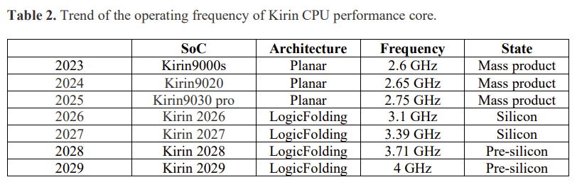
After comparing the two versions, I'm left with two questions. One is about equipment: who supplied the bonding tools capable of this spec? The paper says only that it is the result of years of process development across a multi-vendor ecosystem. The other is about EDA: designing two wafers as a single chip is beyond what any commercially available EDA tool can do today. The paper acknowledges this, stating only that methodological details will be "published within months." Yet the frequency table shows that the 2027-generation Kirin at 3.39 GHz is already tagged as having physical silicon, meaning this toolchain was up and running inside Huawei long ago — and has been validated on at least two product generations. My personal guess is that this EDA capability was built in-house by Huawei. If anyone has insight on this, I'd welcome the discussion.
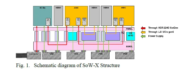
As demand surges for Artificial Intelligence (AI) and High-Performance Computing (HPC), the need for ultra-high integration density and massive data throughput has pushed conventional packaging architectures to their limits. To overcome three critical bottlenecks—reticle size, I/O bandwidth, and thermal management—TSMC unveiled a groundbreaking packaging innovation at the 2025 IEEE ECTC: SoW-X (System-on-Wafer, eXtreme).
This architecture marks not just a leap in packaging capabilities, but a tangible realization of wafer-level system integration. SoW-X redefines how logic and memory interact at scale, opening a new chapter in system co-design and packaging for the next generation of AI and HPC systems.
https://t.co/rhepUjmH1f