I got rejected by Taiwanese universities.
No fancy profile
No perfect path.
Just a diploma student from India with gaps caused by COVID and financial struggles.
But somewhere between late nights, open-source contributions, and learning things alone, I became obsessed with semis
Google outsources merchant verification to BillDesk
- Who ghost devs
-Reject valid docs, and demand bribes (₹25k-4L reported) for "fast" approval. Earnings trapped, apps blocked.
-Google says "not our problem."
I hope I get verified 🤞
Making your first app don't make this mistake like I did
Use posthog free tier like this.
Just focus on these 4 things 👇
- Funnels
Track Open → Sign up → Core action.
1,000 users open but only 200 sign up? Your onboarding is leaking. Fix this first.
- Retention
Check Day 1, 3 and 7. 40% retention with 500 users beats 1% with 10k every single time. This is real PMF
- Session Replays
You get 5k free recordings per month.
Filter for rage clicks or sessions under 30 seconds. Watch exactly where your UI breaks on real Android devices.
- Feature Flags
Use them as a remote kill switch.
New feature crashing the app? Turn it off from the dashboard in seconds. No Play Store review hell.
Do this before you touch A/B testing or fancy pipelines. Get users through the core loop and make them come back. Everything else is noise
@eglitisX Wait what ? You can do that too.
Upload your apps screenshots with your specific niche in the comment add your app name that's it.
Unlimited money glitch
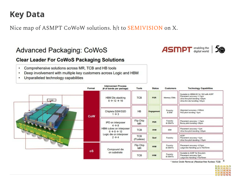
In an advanced packaging technique called “Chip on Wafer on Substrate” (CoWoS) logic (GPU) and memory (HBM) chiplets sit next to each other on a wafer which is then cut into chips and packaged on a high-density substrate
Why there is no pure semiconductor videos from physics to device?
Not enough educational stuff for electronic & robotics
People need to learn more about silicons
Indian students are DIYing a semiconductor fab at IIT Bombay.
In just 10 months they've built:
1. A DLP-based lithography machine.
2. A tube furnace to oxidise silicon.
3. A DC plasma sputter.
Total cost: ₹30 lakh.
Here's a rare behind-the-scenes look at HackerFab IITB.