#Infineon and #NVIDIA are expanding their collaboration on #GaN-based power solutions for 800V DC AI data centers, paving the way for 1 MW+ racks as NVIDIA targets adoption from 2027!💡More: https://t.co/YqdgNxx5L7 🔗
South Korea’s LX Semicon is putting 60+ patents tied to #SiC power semiconductors and epitaxial wafers on the market, signaling a retreat from the sector. With EV demand stuck in the slow lane, pressure is mounting across the SiC sector.💡More: https://t.co/nsD3JibA4q 🔗
AI agents are reshaping server CPU demand! The CPU-to-GPU/ASIC ratio in AI racks is expected to shift from the traditional 1:8 toward 1:2 or even 1:1. 💡 #TrendForce on shifting server architectures and chip ratios: https://t.co/WMt38Kd283 🔗
💰 AI Server Value Climbs on Price, Not Volume.
Combined Capex of the top nine CSPs is projected to keep growing YoY in 2027, inflated by price hikes, part shortages, and prepayments. Pricier next-gen racks and rising memory costs lift ASPs, driving most of the AI server value growth.
What's driving AI server value 👉 https://t.co/p42gbfIFIC
Explore Agentic AI's CPU demand 📖 https://t.co/whddFSecBU
#TrendForce #SelectedTopics
#Intel’s U.S. fab expansion is moving ahead! Arizona’s Fab 62 has begun equipment installation, targeting late-2028 production for potential 18A or 14A capacity, while Ohio One’s first fab begins taking structural shape.💡More: https://t.co/qbqddcPvMr 🔗
Elon Musk says building human-like robot hands is “shockingly difficult.”
Tesla, 1X, and Boston Dynamics are taking different paths: 22 DOF for near-human dexterity, low-gear tendon drives for the home, or four fingers built for mass production.
Inside the US$6B dexterous hand race: https://t.co/WrkO43nYjU 🔗
Rising memory prices and tight foundry capacity boosted #PSMC’s Q3 revenue by 80% YoY and net profit by 338%, with further 10–20% mature-node price hikes planned for 2027.💡More: https://t.co/VFfuobetqo 🔗
#Tesla is reportedly putting KRW 1.1T on the table for AI chip substrates! The deal would lock in Samsung Electro-Mechanics’ FC-BGA supply through 2033, and #NVIDIA is said to be grabbing capacity too. 💡More: https://t.co/IJCdIccn5a 🔗
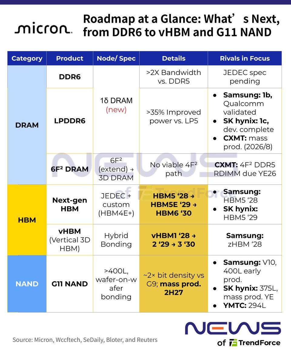
#TrendForce notes that #Micron plans to begin mass producing its 1-delta nm process in 2027, which is set to succeed its current mainstream 1-gamma nm process. Beyond this transition, Micron intends to continue scaling its 6F² architecture before moving directly to 3D DRAM, bypassing the intermediate 4F² architecture. In contrast, South Korean and Chinese DRAM manufacturers still plan to adopt 4F² architecture, highlighting a growing divergence in process technology roadmaps among major suppliers. Micron is also developing memory solutions optimized for AI solutions, including #vHBM and #vEIM, to compete with SK hynix's 3D HBM and Samsung's zHBM.
In #NAND Flash, Micron is preparing to ramp up production of its G11 generation in 2H27. By incorporating wafer bonding and stacking more than 400 layers, G11 is expected to deliver twice the bit density of G9, alongside a targeted 1.5-fold improvement in I/O speed.
#TrendForce believes these advances will enable Micron to close the technology gap with #Kioxia and #YMTC—both early adopters of hybrid bonding architectures—and strenghten its competitive position as NAND performance becomes increasingly critical to an AI-driven market.
Micron’s DDR6 doubles DDR5 bandwidth while LPDDR6 delivers 35% better power efficiency, both built on its upcoming 1δ DRAM node, vHBM goes vertical, and G11 NAND goes beyond 400 layers. 🔗https://t.co/hPuISi998H
#NVIDIA-linked #Groq is reportedly exploring 3D-stacked DRAM for its next-gen AI chips, potentially moving beyond #SRAM as AI models grow larger. Could this reshape AI inference chip design? 💡More: https://t.co/NsxE5uH2cq 🔗
🔥 #Micron has unleashed a wave of memory roadmap updates, spanning DRAM, HBM and NAND. The standout? Its Vertical 3D HBM (vHBM), now with a 2028 mass-production target.
While China's #CXMT pushes ahead with 4F² #DRAM, #Micron is taking the opposite path, sticking with 6F² and arguing that cell architecture alone doesn't determine bit density. What’s next on its memory roadmap? 💡More: https://t.co/8Wnb3NGZYT 🔗
[Breaking] Google Reportedly Sticks With Intel EMIB-T Despite 35% Substrate Yields as HumuFish Schedule Tightens
Uncertainty is growing over potential delays to Google’s TPU v9. Industry sources point to the HumuFish variation as a key area of concern: reported yield problems with Intel’s EMIB-T substrates have raised the possibility of a switch to TSMC’s CoWoS-L. Supply chain checks, however, indicate that HumuFish remains “100%�� committed to EMIB-T.
Yield Gap Raises Production Readiness Concerns
According to Common Wealth Magazine, EMIB-T’s architecture poses two major challenges for substrate suppliers. First, differences in thermal expansion between ABF substrates and embedded silicon bridges make precise alignment difficult during high-temperature processing. Second, NCF (Non-Conductive Film), applied beneath the bridges’ TSVs, can trap air bubbles during bonding, potentially weakening adhesion and further weighing on yields.
Against this backdrop, industry sources say that EMIB-T substrate yields were around 35% in 3Q26, well short of the 50% target set for year-end.
However, efforts are underway. While the reported bottleneck centers on substrate suppliers’ difficulties embedding TSV-equipped silicon bridge dies, industry sources note that Intel has adjusted its substrate electroplating process, while suppliers including Ibiden, Unimicron, and Shinko continue working to improve yields.
With HumuFish not slated for mass production until 1H28, the supply chain still has time to tackle the remaining challenges, according to industry sources.
TPU v9 Packaging Orders Split Between TSMC and Intel
According to industry sources, Google’s TPU v9 lineup is confirmed to include three variants: Broadcom-designed WhaleFish, and MediaTek-designed HumuFish and TriggerFish. WhaleFish is expected to adopt TSMC’s CoWoS-L, with mass production slated for 2H27. HumuFish, meanwhile, is set to enter mass production in 1H28, relying exclusively on Intel’s EMIB-T. TriggerFish is also planned to use EMIB-T, with production targeted for 2H28 or later.
TechNews, citing analyst Ming-Chi Kuo, further explains that TriggerFish is positioned as an upgraded TPU v9 with stronger inference capabilities, designed to address both CPU and memory bottlenecks. According to Kuo, TriggerFish features three key upgrades over HumuFish: 2–3 times the SRAM capacity, an additional simulation die, and a shift to HBM4E from HumuFish’s HBM4.
HumuFish’s Potential Timeline Slip
Amid recent market rumors of HumuFish’s delay, industry sources indicate that the tape-out of Google-designed Compute Die A, built on TSMC’s N2 process, has been pushed back to late October, while other dies remain on schedule.
Against this backdrop, industry sources suggest the delay is expected to push back trial production of the complete package. Commercial Times further notes that the Google TPU v9 project (HumuFish) involving MediaTek could see its tape-out pushed back to January 2027 due to design revisions, potentially delaying shipments until 1Q28.
Taken together, HumuFish’s 1H28 mass production target still gives the supply chain time to work through EMIB-T’s remaining issues, but a tape-out that slips to January 2027 could compress that cushion. How quickly substrate yields climb, and whether design milestones hold, will determine if HumuFish stays on schedule. The outcome will also be a key test of Intel’s ability to win large external customers for advanced packaging.
More details: https://t.co/WxsuIwueKv 🔗
#NVIDIA’s new #CPO prototype moves optical engines from the package substrate onto the interposer, potentially boosting bandwidth density. Could this early-stage design shape Team Green’s future AI interconnects? 💡More: https://t.co/7prHYZlBb3 🔗
#Micron Taiwan's Taoyuan union announced a 24-hour strike from 9 a.m. on Oct. 22 after talks with the #Memory maker ended without agreement; the company said it signed a deal with its Taichung union the same day.💡More: https://t.co/qNVE0nPCn0 🔗 $MU
AI is driving a wave of foundry expansion! TrendForce maps 8-inch and 12-inch capacity by region and new-build plans, including 17 new TSMC phases in Taiwan.
Read more: https://t.co/AjWae237T4 🔗
#Apple is putting up to $100M into U.S. titanium over three years! Alongside partnerships with #TSMC Arizona, Broadcom, and Corning, U.S. firms now produce nearly 100 components for the #iPhoneDuo and iPhone 18 Pro.💡More: https://t.co/rStmG9bT6w 🔗
👀 AI demand may be fueling NAND upgrades, but #YMTC is adding pressure. As the Chinese rival closes the technology gap, #Samsung and #SKhynix face a tougher balancing act: keeping their China fabs competitive while navigating U.S. export curbs.
With roughly 30–40% of their NAND output tied to China, #Samsung and #SKhynix are racing to upgrade local fabs as #YMTC closes in—reportedly producing 294-layer NAND in limited volumes.💡More: https://t.co/zJAjCNXbTy 🔗
Fudan University spin-off Nexilumen has achieved ~201 Gbps/mm² data-rate density in #MicroLED optical interconnects using wavelength multiplexing. The company is now developing systems with hundreds of channels.💡More: https://t.co/7TRHU9dJRb 🔗
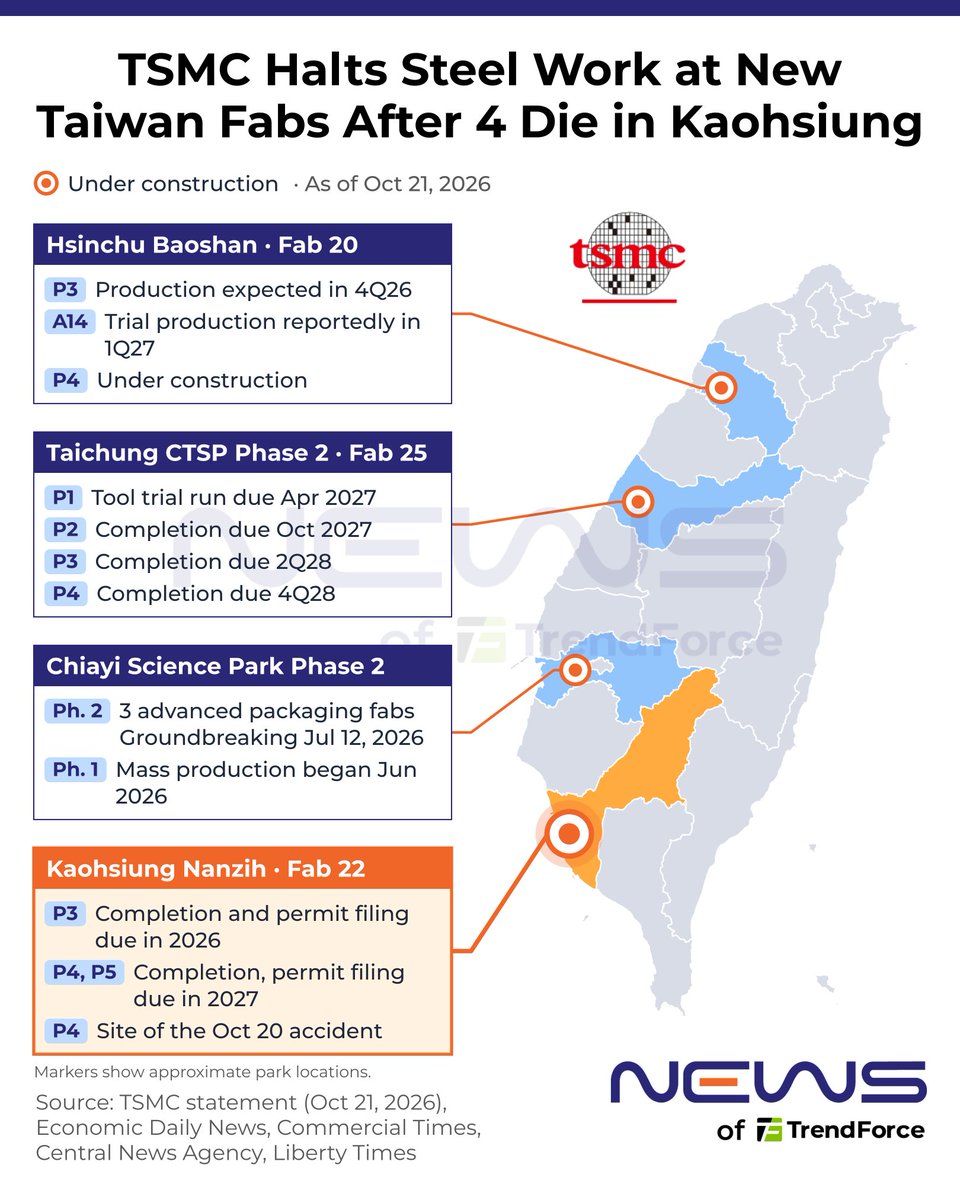
#TSMC has voluntarily halted steel-frame work at all new #Taiwan fab sites after four workers died at its #Kaohsiung Fab 22 Phase 4 construction site on Oct 20; it says it is working with authorities on the cause of the #2nm hub accident.💡More: https://t.co/qNVE0nPCn0 🔗 $TSM