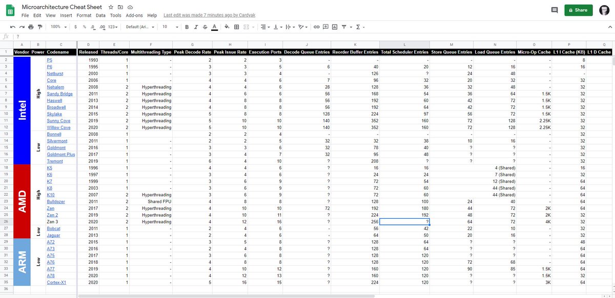
Inspired by @InstLatX64, today I'm introducing the #SiliconGang Microarchitecture Cheat Sheet: https://t.co/jMrjm6RfyX
This can be viewed by all, and it offers centralised information about CPU μarch design such as caches, buffers, instruction width, etc.
Some notes below:
...instruction window, exposing a new, medium-grained parallelism, orthogonal to traditional ILP and TLP. LoopFrog monitors data dependencies between executing threadlets, forwards data for true dependencies and squashes speculative threadlets on ordering violations.
3/3
This is a nice trick called LoopFrog
https://t.co/bX7972RStZ
Using an LLVM-based compiler to insert hints, we achieve a geometric mean loop speedup of 43%, translating to whole-program speedups of 9.5% on SPEC CPU 2017 benchmarks, with only modest area and power overheads.
1/3
LoopFrog runs multiple loop iterations from a single thread in parallel within the microarchitecture. The core can spawn future loop iterations as new microarchitectural threadlets based on compiler-inserted hints, which can leapfrog execution beyond the parent thread’s...
2/3
https://t.co/LbkEqSSjQ1
"SHADOW: Simultaneous Multi-Threading Architecture with Asymmetric Threads"
"dynamically balances ILP and TLP by executing out-of-order and in-order threads simultaneously on the same core"
Could this be what AheadComputing is working on?
#CPU#μarch
https://t.co/uc810tQNX8
"ATR: Out-of-Order Register Release Exploiting Atomic Regions"
Interesting μarch idea here. Instructions that have finished execution but not been committed yet, and also do not contain conditional branches can free up their PRF entry early
#CPU#μarch
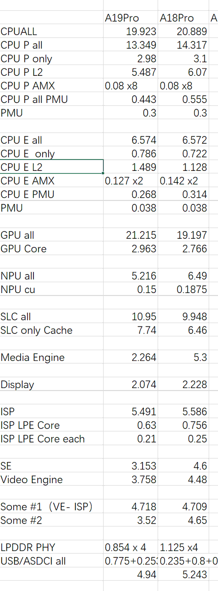
@boris_dg N3P only offers a 6% density gain, so by default it’s not enough to shrink down from the size you mentioned to 99mm.
There’s more to it than that, especially when you remember the CPU and GPU had extra functionality added which increases the transistor count.
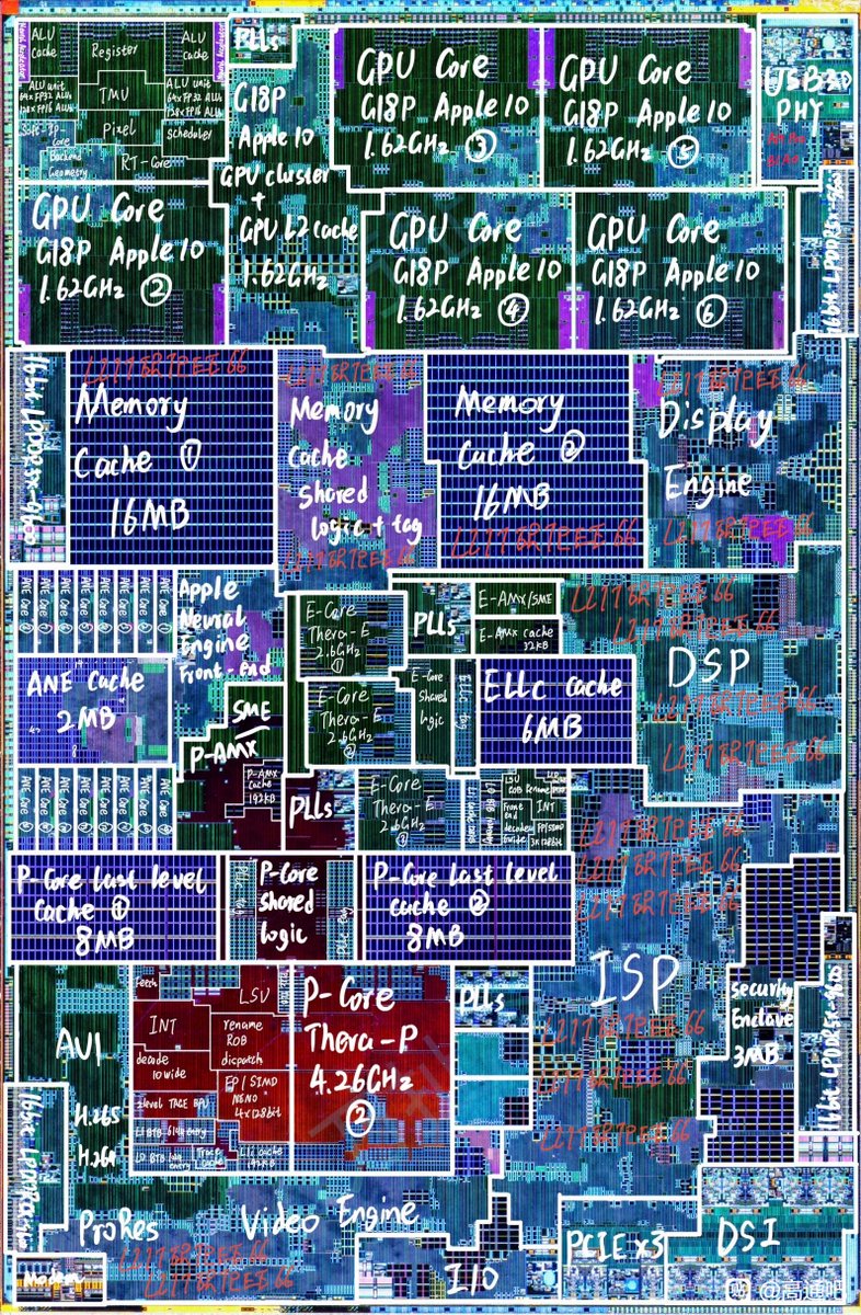
Apple A19 Pro die shot
Die Size 98.68mm²
P-Core 2.966mm²
P-Core with L2 & Shared Logic 5.486mm²
E-Core 0.782mm²
E-Core with L2 & Shared Logic 2.217mm²
SLC 11.026mm²
Somehow looks to be smaller than the A18 Pro (~104mm²)
#Apple#iPhone#CPU#A19
https://t.co/OHqDtnIcko
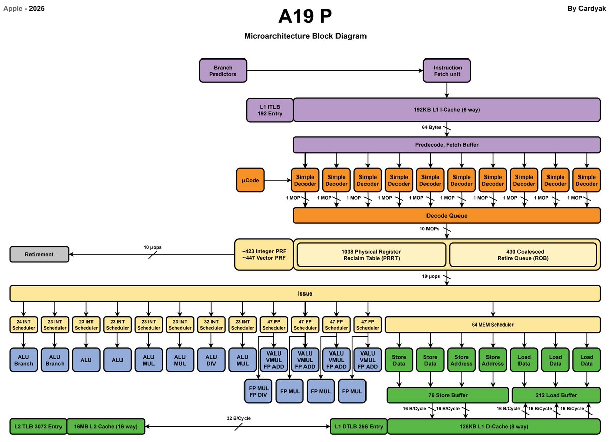
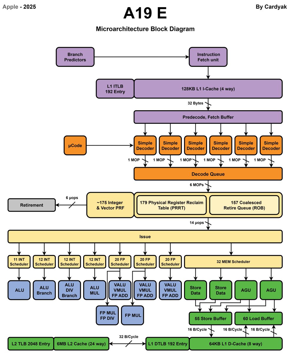
Updated the Apple core diagrams to properly reflect the unconventional ROB structures that are used
Still lots of work to do, I need to separate the dispatch queues from the schedulers and research/confirm the L1 ICache bandwidth
μarch Block Diagrams: https://t.co/cTdkRFDpL1
@MCH2024 There’s also mistakes on their diagram, the ARM documentation tells us there’s 6 FP execution units, not 5. We know this for a fact.
Also the ROB increased by up to 25%, so it can’t be above 960
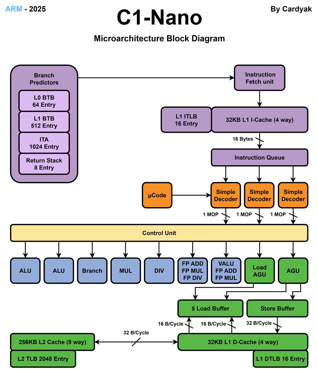
ARM's new μarches added to the block diagram repo
Scarce info this year, these diagrams will be updated and mistakes corrected once more devices are released
μarch Block Diagrams: https://t.co/cTdkRFDpL1
μarch Cheat Sheet: https://t.co/sUmiiw4Ldw
#ARM#CPU#MicroArchitecture
.@Apple A19 SoC chip analysis based on images by @chipwise_tech: 2 P-cores with 8MB shared L2$, 4 E-cores with 4MB shared L2$, a 8-core NPU (Apple calls it 16-cores), 2x 6MB System Level Cache (SLC) and a 5-core GPU. All on TSMCs N3P and smaller than the previous A18.
@divBy_zero@handleym99@MrMadbrain Interesting confession! I assume it saved enough area to be worth the compromise? How easily do you think ARM can expand the decode/allocate stage to 12 or even 16 wide?
Block diagrams for A19 P & A19 E by Apple.
Info sourced by Geekerwan and the Apple Silicon Optimization Guide
μarch Block Diagrams: https://t.co/cTdkRFCRVt
μarch Cheat Sheet: https://t.co/sUmiiw4dnY #ARM#CPU#ARM#Apple#A19#CPU#MicroArchitecture