💠Government of India creating enabling environment for Semiconductor Design Community with direct access to National Chip Design Infrastructure
💠ChipIN (CDAC), one-stop centre for chip designers nationwide, gets momentum with extended support from semiconductor industry leader Siemens EDA
💠20,000+ students from over 250 academic institutions gaining access of EDA tools from Siemens under C2S Programme; ChipIN centre to benefit 85,000 B. Tech, M. Tech, & PhD Students in 5 years
💠Companies approved under the DLI Scheme & C2S Programme to also gain access to Veloce hardware verification solution from Siemens at C-DAC Trivandrum
💠Compute facility to feature 128 CPU cores and a capacity of 640 million gates, helping them address their SoC validation challenges
Read here: https://t.co/xuSxtSJpAO
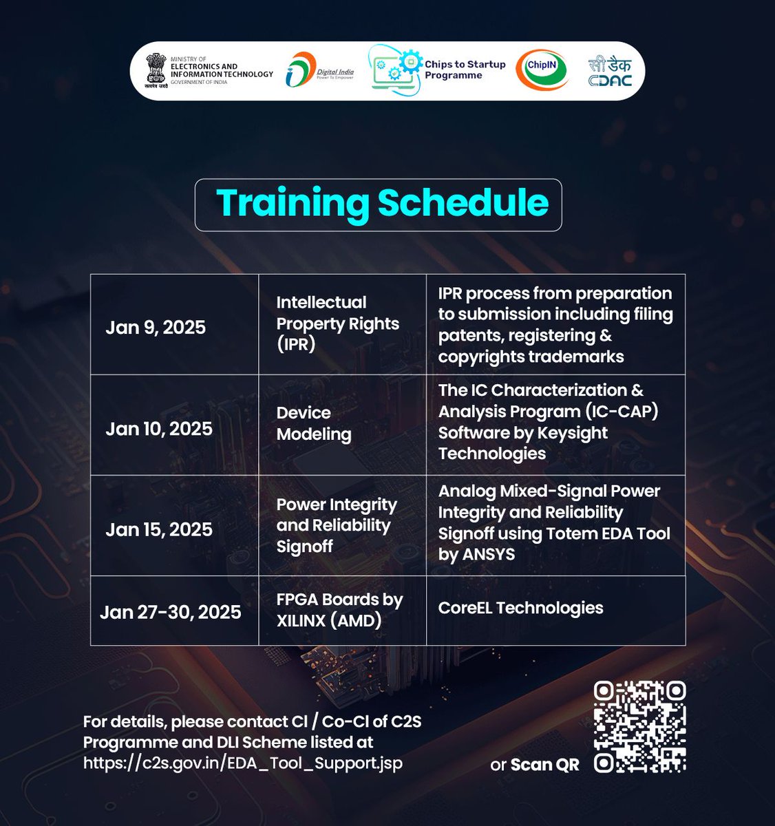
📢@ChipIN_GoI 🇮🇳 invites students, faculty members & engineers from 300 organizations supported under #C2S Programme and #DLI Scheme for training on solutions from Keysight Technologies, ANSYS, XILINX (AMD) and IPR.
🌐More details at https://t.co/NloMgSFab6
#ISM#SemiconIndia
📢 Design Linked Incentive (DLI) Scheme invites proposals from domestic start-ups/ MSMEs for Module Design in identified areas of Wireless and IoT.
🚀 For support on other resources under DLI Scheme, please apply now at https://t.co/7ETB9MZ3c8
#ChipsforViksitBharat #IndiaTechade
📢 Kickstart your SoC design journey with silicon-proven #IP Cores from @Synopsys now made available by @ChipIN_GoI 🇮🇳 for domestic Start-ups and MSMEs under the #DLI Scheme!
🚀 Don't miss the chance to accelerate your SoC design's time-to-market with silicon-proven Interface IPs, IP Subsystems, Foundation IPs, Processor Solutions, Security IPs etc.
🎯 Time to be a #futureDESIGN Start-up is now at https://t.co/7ETB9MYvmA
#DigitalIndia #ChipsforViksitBharat #IndiaTechade
@aartjandegeus
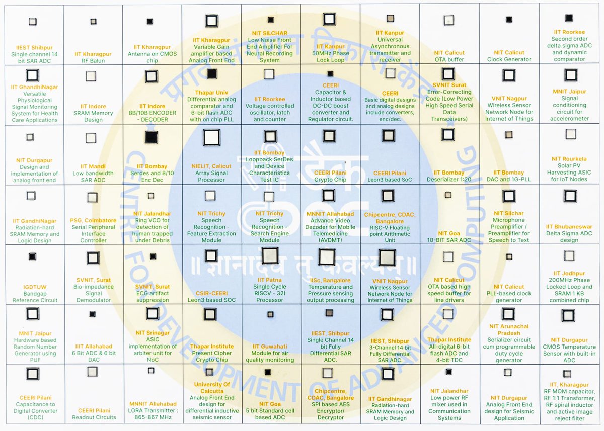
📢@ChipIN Centre 🇮🇳 announces MPW (Multi-project Wafer) Shuttle-I for fabrication of designs by 113 organizations under C2S (Chips to Start-up) Programme at 180nm, SCL (Semi-Conductor Laboratory) Mohali. For details, please visit https://t.co/RWF4p8WatN
#ChipsforViksitBharat #DigitalIndia #IndiaTechade
@AshwiniVaishnaw@JitinPrasada
📢 @ChipIN_GoI 🇮🇳 invites for hands-on training on Analog Mixed-Signal #AMS using EDA tools from @Synopsys from June 24-28, 2024
🎯 All students, researchers & faculty members from 150 organizations under Chips to Start-up #C2S Programme are eligible to attend.
🌐 Contact respective Chief Investigator (CI)/ Co-CI at your institution to access the EDA Tools and registration details at https://t.co/6t27b2RzSd
#DigitalIndia #ChipsforViksitBharat #IndiaTechade
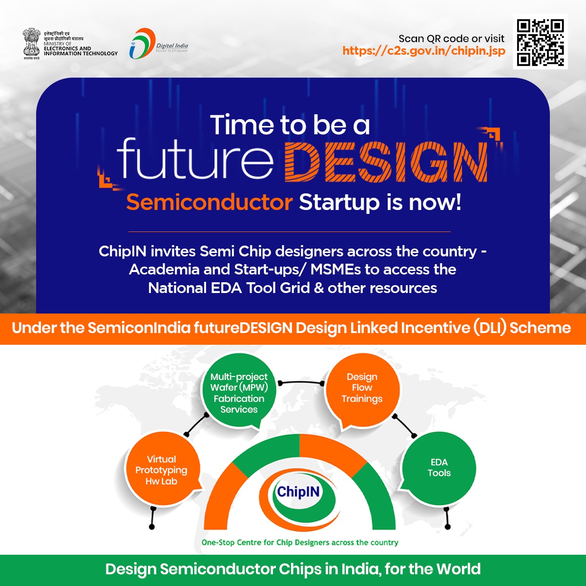
🚀 Design Semiconductor Chips in India 🇮🇳, for the World 🌏
☑️ @ChipIN_GoI invites #Semi Chip designers across India - Academia and Start-ups/ MSMEs to access the National EDA Tool Grid & other resources
☑️ Eligible academia and Start-ups to register for #Semi Chip design support at https://t.co/BbU33U4ook
1. Academia to avail EDA Tools at https://t.co/BZaBcMbArI
2. Start-ups to avail EDA Tools at https://t.co/7ETB9MYvmA
3. Start-ups to avail the financial support for designing #Semi Chips at https://t.co/7ETB9MYvmA
4. Academia & Start-ups to enroll for #Semi Chip design trainings at https://t.co/MJzmy2hhUU
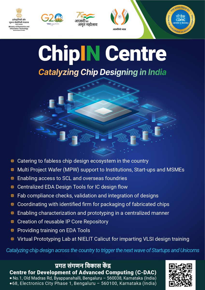
MoS @Rajeev_GoI announces ChipIN Centre at
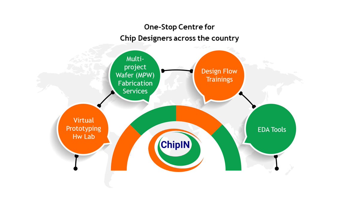
@cdacindia Bangalore; which will act as one stop centre to provide #Semiconductor Design Tools, Fab access, Virtual Prototyping Hw Lab access to Fabless Chip Designers of the country. #SemiconIndia@iiscbangalore
.@ChipIN_GoI setup as a one-stop center at @cdacindia for meeting the semiconductor design and fabrication needs of the Indian fabless designers.
#ChipINInsights shared with 250 chip designers under the Chips to Start-up (C2S) Programme for making use of @Synopsys leading-edge EDA tools (up to 5nm) for designing innovative & complex #Semiconductor circuits.
@Rajeev_GoI@GoI_MeitY #NewIndia #IndiaTechade
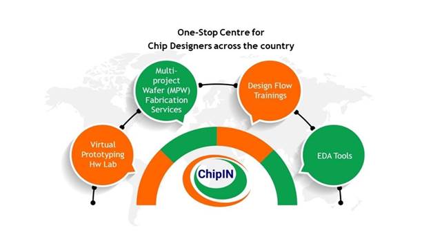
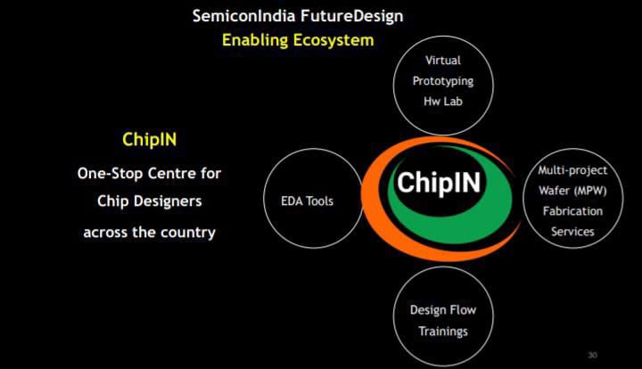
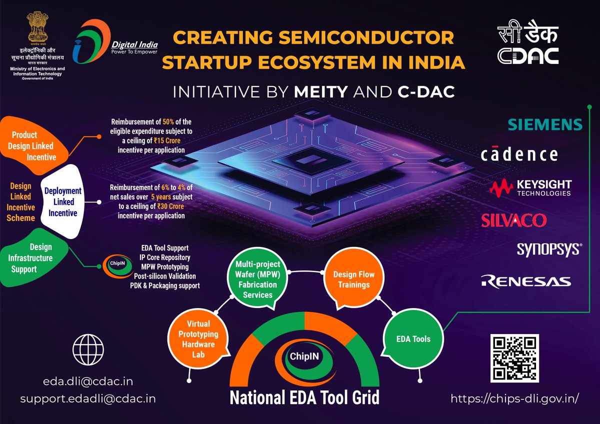
ChipIN Centre at C-DAC Bangalore will act as one-stop centre to provide semiconductor design tools, fab access, virtual prototyping hardware lab access to fabless chip designers from Startups and Academia. It is a common dedicated centralised cloud-supported design facility, not only hosting the most advanced EDA tools for the entire chip design cycle, but also provid aggregate services for fabrication of design at Indian foundries.
https://t.co/wcP2Nyi9WE
@Rajeev_GoI ji this is a very good thing and a stepping stone for India to eventually become a true leader in semiconductors industry . Hope the next Intel or Nvidia comes out of India .
India’s one-stop centre for chip design & fabrication is here!
@ChipIN_GoI setup at @cdacindia, will provide chip design & fabrication support & services to fabless chip designers in the country, which includes:
➡️ Fab Multi-project Wafer (MPW) services at @SclMohali and overseas foundries
➡️ EDA Design tools from leading companies @Synopsys, @Cadence, @Siemens, @ANSYS
➡️ Virtual Prototyping Lab @NIELITIndia using FPGA Boards
➡️ Training on Semiconductor Design flows
@Semicon_India
#IndiaTechade #NewIndia #futureDESIGN