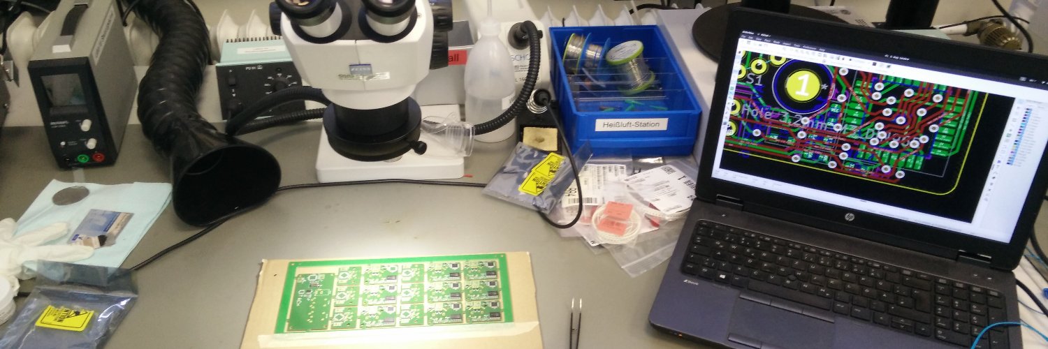
@ptrschmdtnlsn Any particular reason you cannot simply dip the high current trace in more solder for higher cross-sectional area? perhaps even solder in custom bent copper bars as "0 ohm resistors"? I think this is usually how it's done in PSUs.
@blind_via Remember kids, this is what happens when your PCBs don't go visit their dentists regularly. And then when they age they'll have all kinds of issues. Be responsible, teach your PCBs basic oral hygiene.
Wer kennt sie nicht, die Tankstellen, an denen man auch bei Stromausfall weiterhin verlässlich tanken kann? Treibstoff wird mit Eimern aus dem mit bloßen Händen aufgebrochenen Bodentank gefischt und mit Backtrichtern in den Tank eingefüllt. Bezahlung in bar ohne Quittung.
I love both the US and the EU. Both have their strength and weaknesses, and I think it's good we try slightly different routes. We have more in common than not and I find it somewhat sad we focus on what divides us rather than what unites us.
@MacroWorld21@zackslab It's not just the clock speed that matters, slewrate is another key factor in determining the signals bandwidth. Perhaps FETs like really fast driven gates.
@MacroWorld21 No expert, but my best guess is minimizing the overall footprint. They could possibly work just as well "straightened out". But then it'll take up more width on the PCB.