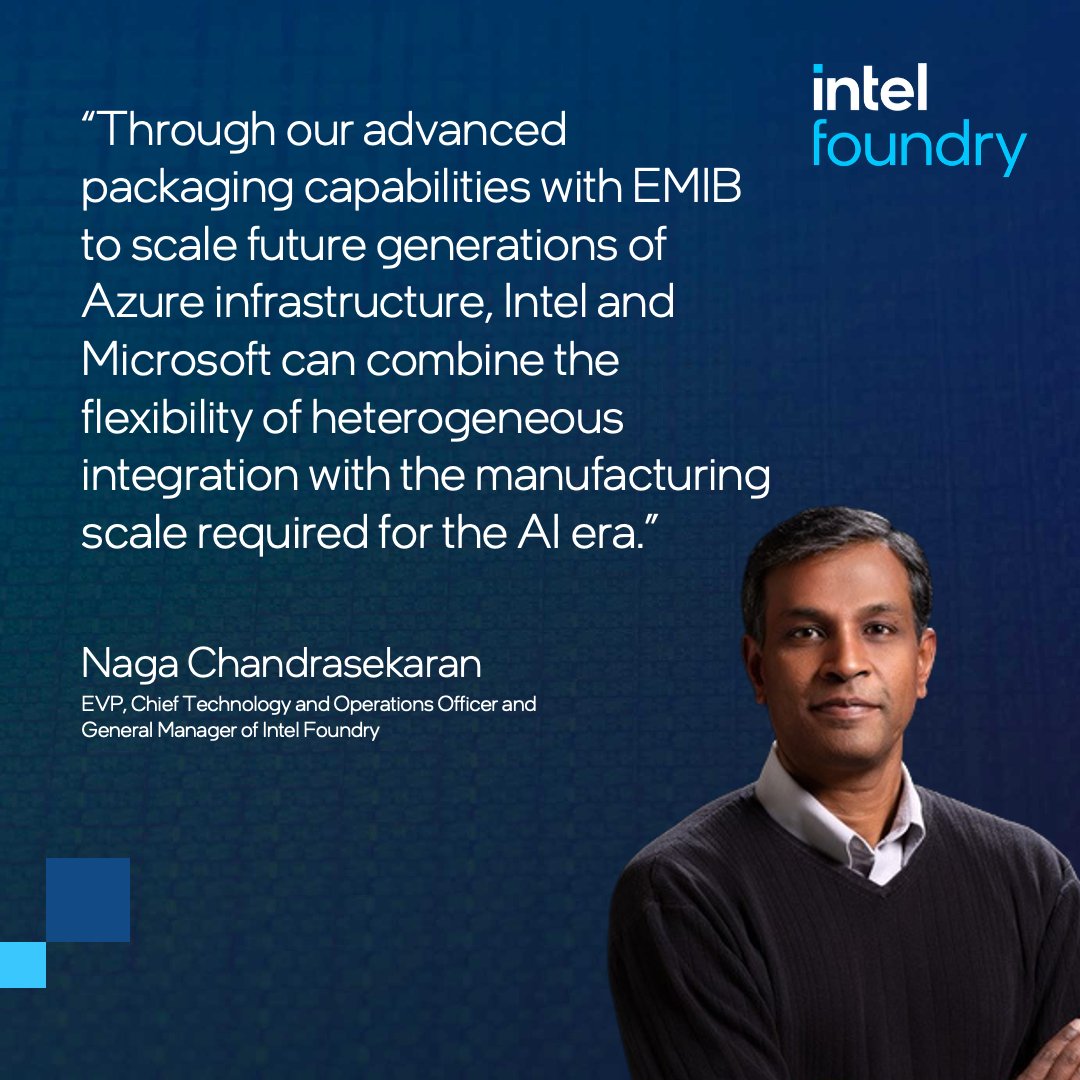
Building semiconductor leadership requires both innovation and the manufacturing capacity to bring it to scale.
In his latest piece, Naga Chandrasekaran highlights Intel Foundry’s growing U.S. footprint, including progress on our Ohio site.
Read more: https://t.co/q0nTRJeQIf
#IntelFoundry
Water stewardship is an important part of sustainable manufacturing.
Through conservation, reuse, and restoration initiatives, Intel has conserved nearly 58 billion gallons of water since 2020.
See the full report: https://t.co/kgBzgnhwig
#IntelFoundry
Intel and @Microsoft share a clear view of the future of AI infrastructure. By combining Intel Xeon and @Azure, we’re ensuring new levels of performance and economics through 2030 and beyond.
@Microsoft and Intel are expanding their decades-long collaboration, with plans to use Intel Foundry's EMIB advanced packaging technology to advance Azure infrastructure for cloud and AI.
Learn more: https://t.co/sE8ZGp8oJl
#IntelFoundry#MSIgnite
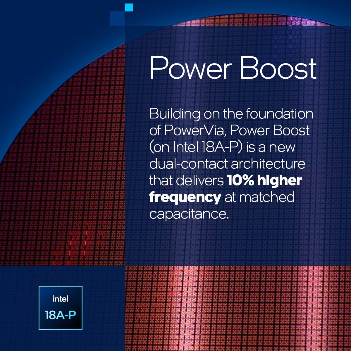
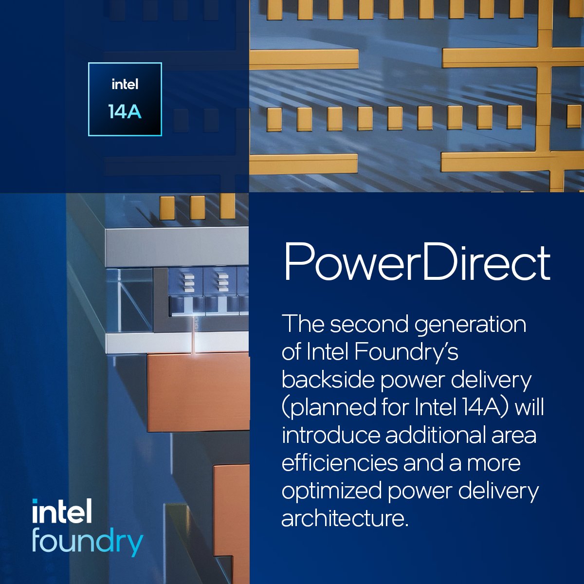
How do PowerVia, Power Boost, and PowerDirect compare?
PowerVia separates power and signal routing on the backside of Intel 18A. Power Boost adds a dual-contact architecture for Intel 18A-P. PowerDirect advances backside power delivery on Intel 14A with greater area efficiency. https://t.co/76JweBXVja
#IntelFoundry
Intel’s investments in Ohio are part of a broader commitment to strengthening U.S. semiconductor manufacturing. From expanding leading-edge capacity to supporting suppliers and local communities, these efforts are helping build the foundation for America’s semiconductor future. https://t.co/i86Ql0QvPp
#IntelFoundry
Designing for Intel 18A-P and Intel 14A? @Keysight has certified its RFPro electromagnetic design software for both process technologies, helping designers validate simulations and reduce design risk before manufacturing.
Learn more: https://t.co/NYZ7iGxfkp
#IntelFoundry
"From a customer perspective, the PDK 0.9 gives customers the confidence to design products on Intel 14A, as the technology is reaching the industry-standard performance and yield maturity expected at this stage of development, supported by silicon-backed validation." - Ben Sell, CVP and GM leading the front-end technology development for Intel Foundry.
Explore our FAQs for more on Intel 14A, including key technology details and milestones on the road ahead. https://t.co/QREiNdBH72
#IntelFoundry
Intel’s impact in Oregon goes beyond semiconductor manufacturing. From developing future industry talent to advancing water conservation and supporting local communities, we’re helping shape a more sustainable future.
Learn more: https://t.co/Xsnswc5W8r
#IntelFoundry
What's happening across Intel Foundry?
Hear from Naga Chandrasekaran on America's semiconductor future, go behind the scenes of our Oregon R&D operations, and explore the latest in AI chip innovation, Intel 14A, EMIB and Foveros.
Catch up here: https://t.co/HcdCWmOhAl
#IntelFoundry
#ICYMI: Semiconductor leadership takes more than innovation. It takes the capacity to bring it to scale.
Naga Chandrasekaran shares how Intel Foundry is connecting U.S. research, manufacturing, and advanced packaging to help shape the future of computing.
Read more: https://t.co/gh5scwC5es
#IntelFoundry
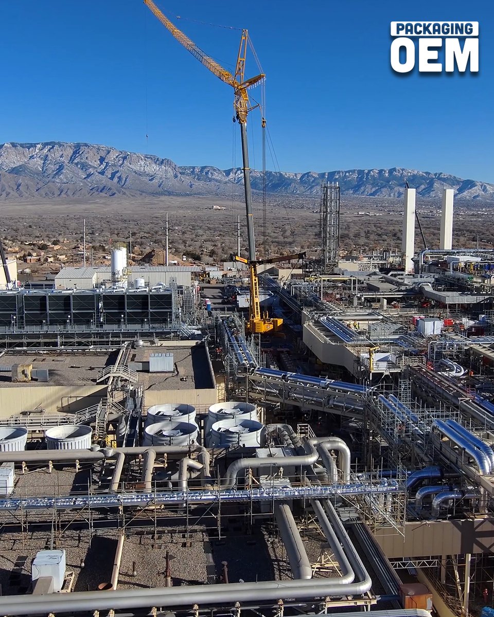
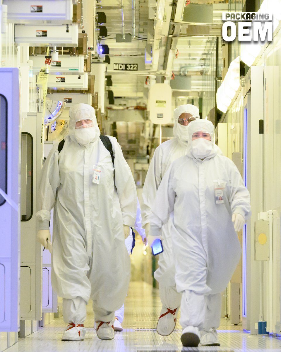
Larger AI chip packages are driving equipment changes at @Intel_Foundry's Fab 9 in New Mexico, where upgraded material handling systems move larger, heavier carriers.
Read more ➡️ https://t.co/S01sxsYrcX
@intel#ai#madeinusa
Arizona is helping shape the future of semiconductor manufacturing. From manufacturing innovation to workforce development, Intel is strengthening the semiconductor ecosystem and supporting local communities.
Learn more: https://t.co/O2IulLhQgW
#IntelFoundry
As chips get smaller, innovation requires more than simply shrinking transistors.
From planar transistors to FinFETs and gate-all-around architectures, bringing these technologies to life relies on extraordinary manufacturing precision.
Explore the engineering behind these innovations and see what's next for semiconductor technology in our full conversation on @dwarkeshpodcast: https://t.co/3CLvUqmT3x
Advancing semiconductor performance isn't just about smaller transistors.
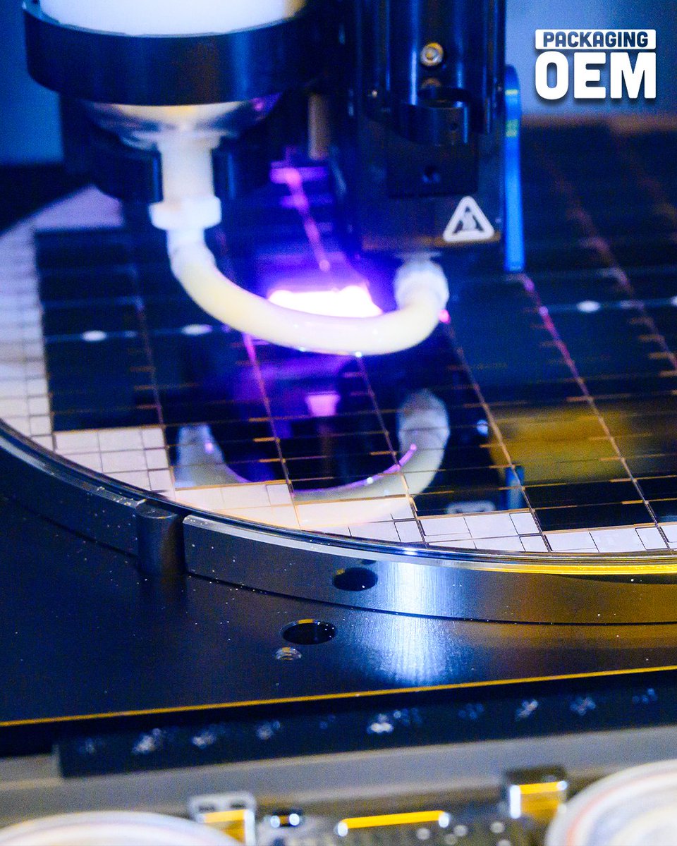
Innovations in advanced packaging, like hybrid bonding, enable denser chip-to-chip connections and create new opportunities for performance and power efficiency. But bringing these technologies to life requires extraordinary manufacturing precision.
Discover the engineering behind next-generation semiconductor packaging.
Watch the full conversation: https://t.co/ymlh3GguH8
#IntelFoundry
What does it really take to make the world's most advanced chips?
Thousands of intricate manufacturing steps. Extraordinary engineering precision. And an industry working to meet growing global demand for computing.
Get an inside look at Intel's semiconductor innovation as Chris Auth, Pushkar Ranade, and other Intel experts join @dwarkeshpodcast to explore the science, technology, and manufacturing expertise behind advanced chips.
Watch the full conversation: https://t.co/KWt9uynnFY
We’re raising the roof on the first fab in Ohio.
The initial major structural truss is going up at the Intel Ohio site, marking another step toward strengthening U.S. semiconductor manufacturing leadership.
Read more: https://t.co/35WXwHi4mc
#IntelFoundry