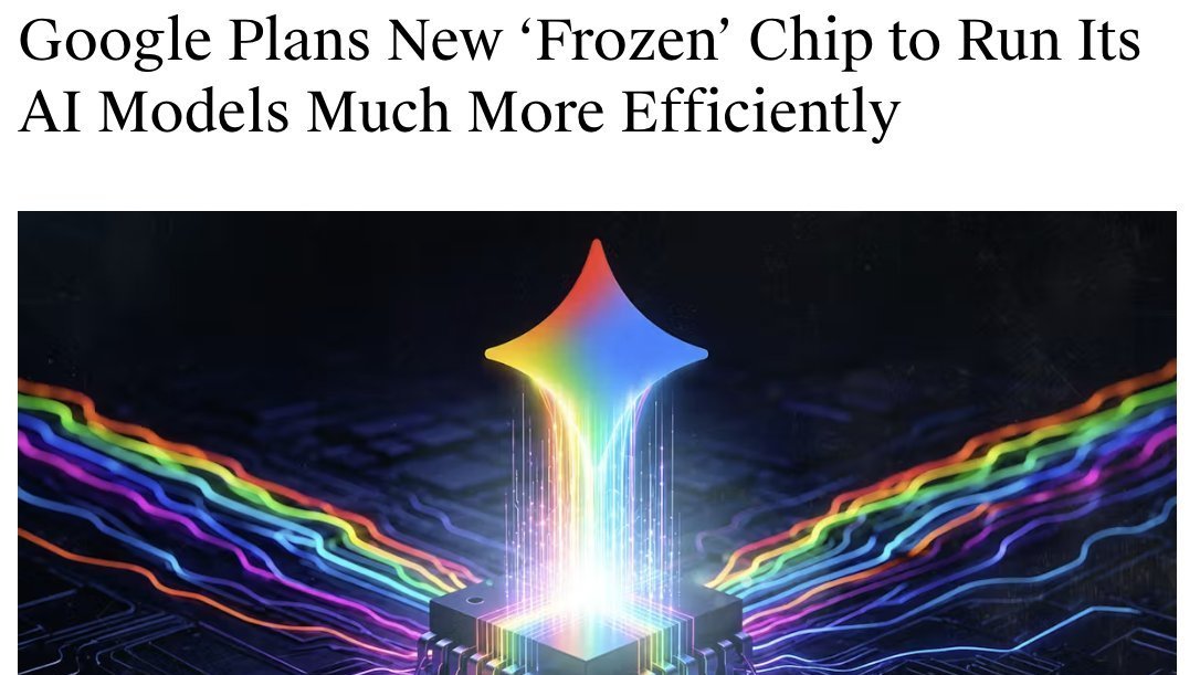
$GOOGL Google is planning a new chip called “Frozen v2” and will likely be fab'd at $INTC Intel Foundry.
This is basically a custom inference ASIC with big chunks of the Gemini architecture baked straight into silicon. The goal is for 6-10x better efficiency than their latest TPUs by cutting data movement and unnecessary decisions.
Google is already moving real TPU production to Intel. Reports from June say they ordered Intel Foundry to make over 3 million TPUs for 2028, which could be roughly half of what they plan to build that year.
$TSM capacity is jammed with AI demand, so hyperscalers are splitting volume. Intel’s 18A node is now in high-volume production (their own Panther Lake and Xeon chips are already on it), and their EMIB-T packaging is specifically strong for these big, HBM-heavy AI accelerators.
Frozen v2 or the next TPU generation (v8 series) ending up on Intel silicon aren't rumors anymore - big FYI.
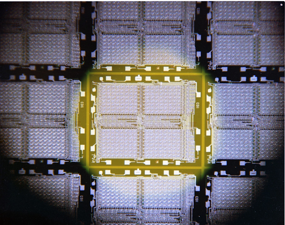
Only few people may now be aware that @intel has been a memory technology pioneer since its founding in 1968:
1969: Intel's first product was a 64-bit Schottky bipolar static RAM, the world's first solid-state memory chip that helped move the industry from magnetic core to semiconductor memory.
1970: Intel shipped the first commercially successful DRAM chip (1 kbit 1103) and quickly displaced magnetic core memory in many systems.
1971: Intel invented Erasable Programmable Read-Only Memory (EPROM), which allowed users to program and erase code using ultraviolet light.
1988: Intel pioneered NOR flash, launching the first commercial NOR‑type flash chip in 1988 as a successor to EPROM for code storage.
2015: Intel introduced 3D XPoint, a new non‑volatile memory technology positioned as a distinct “third category” between DRAM and NAND flash in terms of speed, endurance, and density.
A love-hate relationship with memory, but memory innovation is in the DNA of intel.
Thank you for the memories!
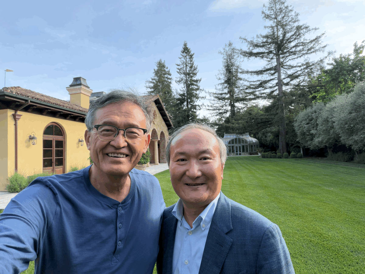
Super excited to welcome my close friend Seok-Hee Lee back to Intel! @seokhee4 is a highly regarded semiconductor process integration expert and successful CEO (SK Hynix). Early in his career, he spent over 10 years at @intel, contributing to several critical Intel process technologies. He will now oversee our advanced packaging technology development and drive exciting new system integration projects! Advanced packaging and system integration are increasingly critical areas for Intel Foundry and for the future of computing. Seok-Hee will help Intel accelerate the ramp of our industry leading EMIB-T and HBI technologies. I look forward to partnering with him and have him rejoin Intel at this critical time!
https://t.co/DfPaWAWMZM