میرے انٹرویو اخبار میں۔
My interview in newspapers. Regarding supply chain for Silicon wafer for Pakistan semiconductor ecosystem.
https://t.co/XXIp1gfFgZ
🚨🇨🇳 China’s AI future gets domestic chip power boost
Four cutting-edge AI models—all trained on homegrown Chinese hardware—are already in the pipeline, the South China Morning Post reports
The lineup consists of:
🔸 GLM-Image (Zhipu AI): an image generation model powered by China’s Ascend 910 AI accelerator
🔸 LongCat-2.0-Preview (Meituan): built on a domestic cluster with over 50,000 locally made chips
🔸 BitCPM-CANN (ModelBest): created to run directly on smartphones and PCs, this efficient model was trained using Huawei's Ascend chips.
🔸 EvoPhys-World (Peking University): A 5D world model designed for physical-space movement, trained on China’s MTT S5000 chips
This coordinated leap not only diversifies China’s AI ecosystem but also boosts its technological resilience—directly countering America’s aggressive semiconductor restrictions
Sony & imec just scored a big lithography win — self-aligned TSVs that boost overlay tolerance by 3x.
The challenge with large TSVs is threading the needle between the ultra-tight MOL vias at the smallest critical dimensions. Overlay tolerance is razor-thin there, but they’ve developed a clever self-aligned scheme that dramatically improves device yield.
Even better, this lets them enlarge the TSVs below the MOL stack, which slashes resistance, improves timing, and further lifts yield.
Very cool process tech!
🚨🇨🇳 China turning giant diamond wafers into AI power advantage
China is rapidly scaling production of ultra-large synthetic diamonds that could solve one of AI's biggest bottlenecks, namely, heat, the SCMP reports
🔸 Chinese researchers have expanded single-crystal diamond wafers from a few millimeters to 8 inches (20.3 cm), approaching basketball-sized dimensions
🔸 Diamond conducts heat at over 2,000 W/mK — more than 5x better than copper, making it ideal for cooling next-generation AI chips
🔸 China has built a largely self-sufficient ecosystem spanning diamond growth, manufacturing equipment, materials engineering and commercial deployment
🔸 Diamond thermal-management technology could improve computing performance by around 10%, Chinese researchers stressed
As AI competition increasingly shifts from software to hardware, breakthroughs in advanced materials may prove just as important as breakthroughs in chips themselves
China is deliberately choking the global supply of Indium Phosphide (InP), the material that makes every laser in every AI data center work.
Reuters confirmed: US officials have visited China multiple times to resolve this. China is still blocking export approvals on purpose. They want to maintain the bottleneck.
Chinese producers like Yunnan Germanium (https://t.co/wyCjVX0HNv) and Guangdong Xiandao are scaling capacity fast (Yunnan investing $28M to reach 450K wafers/year, shipments up 74% in 2025). But even if export approvals are granted, overseas shipments will be "limited."
Switching InP suppliers requires lengthy qualification cycles. You can't just find a new source overnight. 12-18 months...
This will help explain the recent price action in the below names.
WINNERS:
$SIVE.ST CW lasers ARE InP devices. Policy-duration shortage extends their 14-quarter laser supply constraint indefinitely. Every month China maintains this, SIVE's pricing power widens.
$LITE Substrates come from Sumitomo + JX Advanced Metals in Japan. Entirely outside the China export gate. Their competitor's supply gets squeezed while theirs is control-immune. This is the cleanest relative advantage.
Win Semi (https://t.co/la0Q2W86G1) Only pure-play III-V foundry on earth. InP wafer fab capacity is scarce globally. Tighter substrates = their existing capacity commands higher pricing.
$AEHR Sole-source wafer-level burn-in testing for InP and SiPh devices. When every wafer is more valuable because the input material is scarce, the cost of shipping a bad one goes up. Testing intensity rises with scarcity.
AIXA (https://t.co/B1hBTJxtCC) Makes the MOCVD equipment needed for InP epitaxy. Every country trying to build domestic InP capacity needs their tools. More fragmentation = more equipment orders.
$SOI.PA Photonics-SOI monopoly. InP scarcity makes the entire optical layer more expensive, increasing the value of every component in the stack including Smart Cut SOI wafers.
LOSERS:
$COHR Reuters specifically names Coherent as "mainly supplied by AXT." AXT manufactures IN China, inside the export gate. Even if approvals come, shipments will be limited. COHR carries a substrate risk that LITE does not. And switching requires lengthy qualification cycles.
$AAOI Demand is not the issue; laser/EML/InP component supply is. If AAOI cannot secure enough laser chips, capacity ramp can slow.
$AXTI AXT is a US-listed InP substrate maker that manufactures in China. Their entire equity value is an export-approval question. If approvals flow, massive upside. If they don't, the business model breaks for Western customers.
We are watching real-time supply chain warfare over AI supremacy. The companies that own the physical bottlenecks in this chain benefit every time the world fragments.
🚨🇨🇳 China cracks code for affordable optical chip manufacturing
Hangzhou-based micro and nanomanufacturing company Prinano says it’s created nanoimprint gear that can mass produce optical/photonic chips for 1/10 the cost of the millions-apiece ASML-made ultraviolet lithography machines
The equipment, known as the PL-AS vacuum air-cushion nanoimprint lithography (NIL), can create “customized double-layer imprinting materials and core processes” on advanced industry standard 8-inch wafers
These chips’ uses are legion and include:
🔸 data center and telecoms equipment
🔸 high-performance and quantum computing
🔸 automotive LiDAR
🔸 optical biosensors for healthcare applications
SCMP says the breakthrough, if verified over time, could prove a massive boon for China’s domestic electronics industry amid the ban of the sale of some advanced models of Dutch-made ASML equipment to the Asian nation
Besides technological sovereignty, Prinano’s new equipment means massive cost savings, equivalent to billions of dollars, the unlocking of new domestic and foreign markets and greater affordability for industrial and consumer applications
Prinano says it delivered its first semiconductor NIL system to a local customer last August. The next step should be mass production
What happens when nuclear technology goes modular? ⚛️
Advanced light-water SMRs deliver 50 to 350 megawatts of power using proven pressurized or boiling water reactor technology.
Google DeepMind CEO:
"The gap between people who use AI and people who don't will be the largest skill divide in human history"
Demis Hassabis spent 50 minutes at Stanford saying things most CEOs would never say publicly
this is exactly the kind of conversation people pay $250,000 to be in the room for
if you want to stay competitive, understanding AI is no longer optional
I wrote a full guide on Claude features 99% of people don't know exist
watch this video, then read the article below
those two things alone put you ahead of most people using AI right now
Recently, CETC 48th Institute has developed its 1st high power diamond MPCVD prototype which has entered customer validation period.
MPCVD is dominant production method for electronic-grade synthetic diamond.
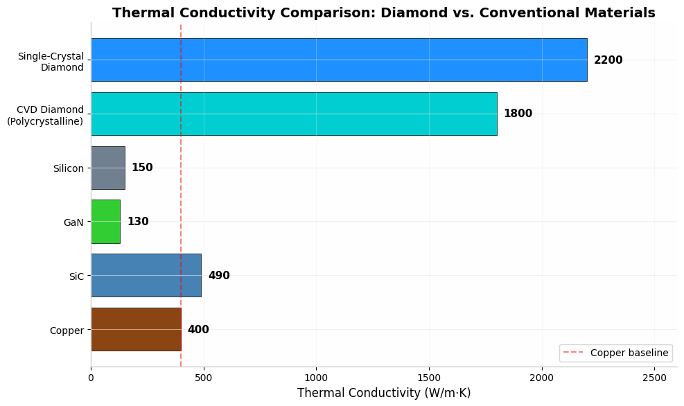
Single crystal diamond has thermal conductivity of 2200 W/m·K, significantly higher than conventional Copper (400) or Copper-Diamond (600 to 1000+). The latter is now entering service on consumer electronics device, EVs & AI-chips.
Single crystal diamond with its even higher thermal conductivity is the ultimately substrate of GaN RF chips, photoconductive switches, Power Electronics & laser diodes.
There are many huge players in diamond industry in China from 惠丰钻石 to 超晶热导 to 国机精工 & CAS, producing equipments, tools, wafers & diamond powder.
AI is just one of many industries where 4th generation semiconductor material is necessary.
Chinese memory module makers ramp up production as CXMT DDR5 breakthrough hits market. https://t.co/ZVR4qzupM9 The Hefei-based company said its DDR5 chips supported speeds of up to 8,000 Mbps and die densities of 16Gb and 24Gb, targeting servers, workstations and PCs.
🇨🇳 China shatters world record in quantum computing
Researchers at the University of Science and Technology of China have unveiled Jiuzhang 4.0 — the latest prototype of their quantum supercomputer.
Jiuzhang 4.0 can manage 3,000 photons — a dramatic leap from the 255 photons handled by its predecessor — signaling major advances in photon generation, optical circuitry, and error management.
Tested on Gaussian Boson Sampling, Jiuzhang 4.0 completed the model in just 25 microseconds — a task that would take a classical supercomputer longer than the age of the universe to solve.
China just unveiled Jiuzhang 4.0, a programmable photonic quantum computer that completed a Gaussian boson sampling task in 25 microseconds.
Researchers say the world’s fastest classical supercomputer would need more than 10^42 years.
While one civilization is quietly building the next generation of computing power, Washington keeps adding Chinese high-tech companies to its blacklist.
The U.S. tries to “win the future” through containment.
China keeps manufacturing pieces of it.
Photons.
Quantum states.
Cryptography.
AI.
Next-generation computing.
This is infrastructure for the next century.
UNDERSTANDING GaN vs. SiC
Lately investors new to semiconductors and new to power electronics have been asking me about "GaN vs. SiC." There is no GaN vs. SiC.
Power semiconductors are defined by two variables: voltage blocking capability and switching speed. These trade off against each other, and different applications sit at different points on that curve.
SiC is the right material for high-voltage, high-power applications where switching speed matters less than raw blocking capability. Utility-scale solar and very large (larger than 50 MWh) battery systems should often be served by SiC because their value driver is primarily the energy content.
This is also why traction motors (like EVs and locomotives) can use SiC –– the computation environment is relatively simplistic so the slow speeds are acceptable. SiC devices today block up to 10 kV and switch cleanly at those levels. Nothing else does.
The most interesting area of power development, though, is in projects where the value driver is a mix of energy, power, capacity, and harmonics. Like a data center. Or a grid-supporting 5 MWh BESS. Or V2X devices that link electric cars and trucks up to the grid. This requires deft computational power handling.
These are ~all of the interesting next-gen power applications. You serve your local need well (charging the car, powering the data center); but you are also performing ultra high-speed grid support activities.
GaN owns the sub-3 kV space, and it owns it decisively. At voltages below 1.2 kV — consumer fast chargers, server power supplies, EV on-board chargers, microinverters — GaN switches at frequencies an order of magnitude higher than SiC, in a fraction of the package size, at a cost that follows a steep downward curve driven by HVM in consumer electronics. The 140-watt USB-C laptop charger uses GaN switching at a million times per second. A comparable 1990s power supply was four times larger and ran hot enough to need a fan. That cost and density curve is not stopping.
The framework is simple. If your application is above 3 kV and switching speed is secondary to blocking voltage, use SiC. If your application is below 3 kV and you need speed, density, and cost efficiency, use GaN. Between roughly 1.2 kV and 3 kV is contested territory where the answer depends on the specific thermal, cost, and frequency requirements of the design.
The cost trajectories of the two materials reflect their origins. SiC crystal growth happens above 2,000°C at a rate of roughly 100 to 300 microns per hour — a thousand times slower than silicon. Each step up in wafer diameter, from 4-inch to 6-inch to the 8-inch transition now underway, requires reinventing the thermal field and crucible design from scratch. 6-inch SiC substrates fell roughly 30% in price in 2024, driven by Chinese overcapacity, and the move to 8-inch wafers should cut per-die costs another 30 to 40% once yields stabilize — but those gains come hard and slow.
GaN's cost curve is of different stuff entirely. Because GaN-on-silicon grows on standard substrates, it inherits the economies of the silicon ecosystem. 150mm GaN-on-Si wafer prices have fallen roughly 40% since 2020. Prices have crossed below $1 per transistor for high-volume GaN devices. The industry is now moving toward 300mm GaN-on-Si, which will yield 2x more chips per wafer than 200mm. That cost curve is being pulled by billions of consumer electronics units and the grid gets to ride it for free.
GaN does have a ceiling. At medium-voltage grid applications — like 34.5 kV — GaN cannot block the full line voltage directly. This is where GaN challengers go wrong. They presume that the only architecture possible is a direct, centralized, single-device approach to handling large voltages. Not so.
The more interesting path is to keep GaN operating within its native voltage range — below 12 kV — and build the medium-voltage function from an array of GaN-based modules. Each module runs at GaN's switching frequencies, which are high enough that the transformer inside each module shrinks to the size of a paperback. The aggregate system handles medium-voltage grid connection without exposing any single device to voltages it can't block. What you lose in architectural simplicity, you gain in speed, redundancy, cost, and manufacturability — because you're building from parts that already exist in billion-unit volumes on a known transistor cost ramp.
Stacking GaN will do something consequential: bring semiconductor switching speeds to grid scale. And thus bringing a cost profile that follows true high-volume manufacturing economics rather than industrial green-metal-cabinet economics.
But the putative "competition" between these semiconductors isn't a reflection of reality. There isn't a winner, really. The grid needs both materials deployed where each is strongest.
Femtosecond laser machining is a nanometer precision manufacturing method that uses laser pulses lasting only few quadrillionths of a second (10⁻¹⁵) to remove material from an object without collateral thermal damage.
The technique is known as "cold ablation” which allows for the creation of intricate sub-micron structures in almost any material, from metals to hard ceramics, polymers, glasses and even sapphire.
Because the pulses last only 300 femtosecond, the energy released is deposited so fast that cannot be diffuse into the material, the bursts prevent the localized concentrate absorption responsible for deformations or burrs.
The technique is used for precise cutting, engraving and drilling, offering high accuracy, versatility, and minimal waste, ideal for medical, photonic, aerospace, and microchips fabrication.
🔗 https://t.co/Y1me8nXgPM
The Best-Selling Laptop Brands in the World: Annual Units Sold 💻
1. 🇨🇳 Lenovo – 48.5 Million
2. 🇺🇸 HP – 39.0 Million
3. 🇺🇸 Dell – 28.5 Million
4. 🇺🇸 Apple – 23.5 Million
5. 🇹🇼 ASUS – 15.5 Million
6. 🇹🇼 Acer – 14.0 Million
7. 🇹🇼 MSI – 3.0 Million
8. 🇰🇷 Samsung – 2.5 Million
9. 🇺🇸 Microsoft – 2.5 Million
10. 🇨🇳 Huawei – 2.0 Million
11. 🇧🇷 Positivo – 1.5 Million
12. 🇰🇷 LG – 1.2 Million
13. 🇨🇳 Honor – 1.0 Million
14. 🇨🇳 Xiaomi – 0.8 Million
15. 🇺🇸 Razer – 0.6 Million
16. 🇯🇵 Fujitsu – 0.5 Million
17. 🇯🇵 Dynabook – 0.5 Million
18. 🇹🇼 Gigabyte – 0.4 Million
19. 🇯🇵 Panasonic – 0.3 Million
20. 🇯🇵 VAIO – 0.2 Million
Source: IDC, Gartner, Official Company Reports
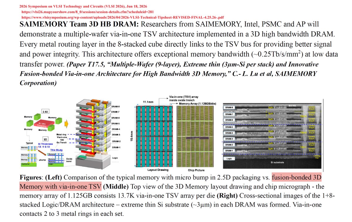
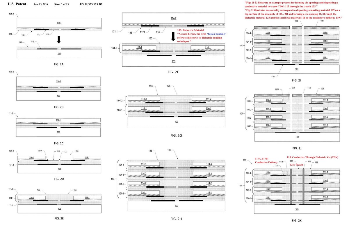
"Microelectronic Assemblies including Stacked Dies Coupled by A Through Dielectric Via", Stephen Morein (CTO, SAIMEMORY, Aug 2025 --), ..., Prashant Majhi, Intel (Jun 2022) https://t.co/hh6alJx32o
<= VLSI 2026 https://t.co/KnYRmN9PSp
ZAM、4月22日 https://t.co/sftnfz2DWD
38億円🤔
India's also making an ASML! Their immersion scanner will cost 10% of what ASML charges and has 1.5x the resolution. How? It doesn't even matter; the whole world wants their own ASML.
h/t @Eveosian