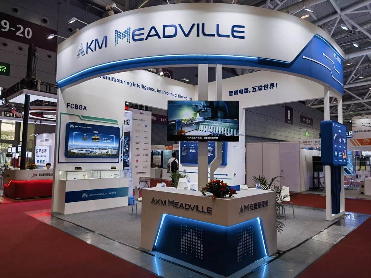
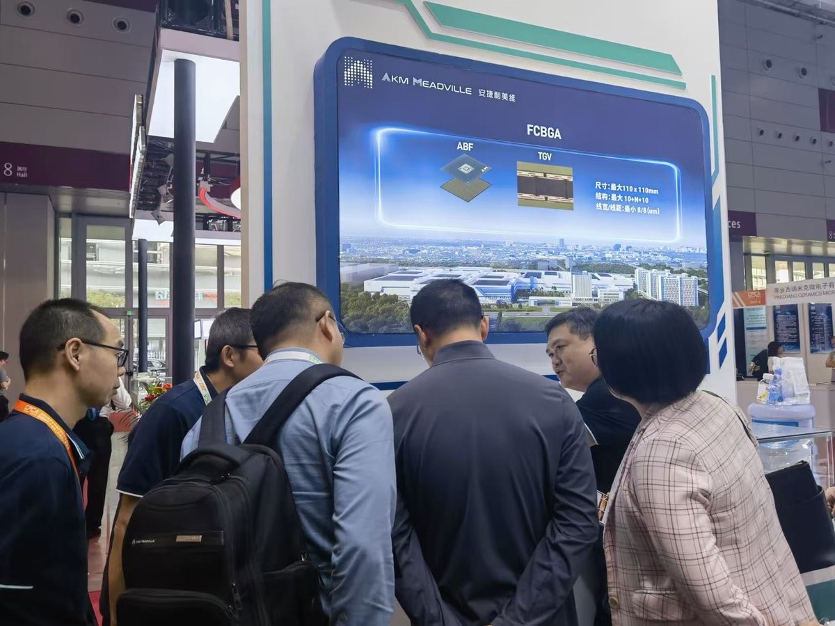
Guangdong Kezhuo Semiconductor is a leading back-end packaging equipment supplier. In 2018, it launched China’s first 12-inch fully automatic wafer dicing machine with ≤2μm precision. The equipment supports traditional packaging, 2.5D/3D stacking, HBM, and FC-BGA.#wesemibay
Guangdong Kezhuo Semiconductor is a leading back-end packaging equipment supplier. In 2018, it launched China’s first 12-inch fully automatic wafer dicing machine with ≤2μm precision. The equipment supports traditional packaging, 2.5D/3D stacking, HBM, and FC-BGA.#wesemibay
South Korea’s AI semiconductor industry is accelerating, with SK hynix expanding HBM and advanced packaging capacity through a KRW 19 trillion investment, increasing demand for semiconductor ceramics, quartz, and silicon-based precision components.
#Semiconductor#wesemibay
iStar Technology specializes in bonding and packaging lithography equipment for HBM and 2.5D/3D Chiplet applications. Backed by the Greater Bay Area’s advanced packaging ecosystem, WESemiBay connects global resources to accelerate advanced packaging and HBM collaboration.
South Korea continues to accelerate its HBM (High Bandwidth Memory) industry expansion, as Samsung Electronics and SK hynix ramp up HBM production capacity, driving strong demand for advanced packaging bonding and lithography equipment. #Chinasemiconductor#wesemibay
South Korea continues to accelerate its HBM (High Bandwidth Memory) industry expansion, as Samsung Electronics and SK hynix ramp up HBM production capacity, driving strong demand for advanced packaging bonding and lithography equipment. #Chinasemiconductor#wesemibay
WESEMiBAY 2026 connects the full semiconductor and AI computing infrastructure value chain, bringing together upstream and downstream enterprises to foster technology exchange and cross-border collaboration.
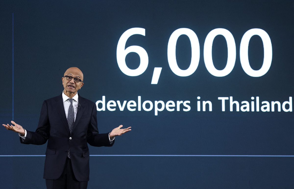
Thailand is rapidly emerging as a Southeast Asian AI Infrastructure hub, driven by major investments in cloud computing, data centers, and next-generation computing infrastructure.
#Chinasemiconductor#wesemibay
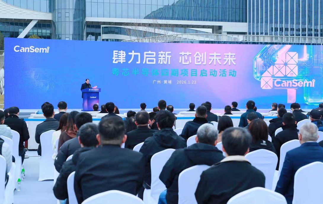
The Greater Bay Area has a strong ecosystem: Shenzhen hosts HiSilicon and Shennan Circuits in AI chips, memory packaging, and substrates; Guangzhou, led by CanSemi, strengthens 12-inch wafer fabrication; Dongguan with Nexperia supports advanced packaging and power semiconductors.
South Korea is accelerating AI data center development, from a 20MW project by OpenAI, Samsung SDS, and SK Telecom to a 100MW facility by SK Group and AWS and a 250MW hyperscale project by Shinsegae Group, marking large-scale AI infrastructure deployment.
#AI#wesemibay
Anjieli launches a $1B advanced packaging substrate park; capacity and output will double upon completion, bringing opportunities for suppliers. This expansion will double capacity & create opportunities for global material & equipment suppliers. #Chinasemiconductor#wesemibay
JCET has strong HBM packaging orders, while Hitech Semiconductor (Taiji Industry) exclusively serves SK Hynix. Their 2026 capacity expansion will bring steady orders for suppliers of TC Bonder, molding compounds and bonding materials. #China#semiconductor#wesemibay
STI Korea launches a $18B power semiconductor base in the Greater Bay Area, phase 1 produces AMB ceramic substrates, reflecting a vibrant market and upcoming business opportunities for equipment and material suppliers. #China semiconductor #WESEMiBAY
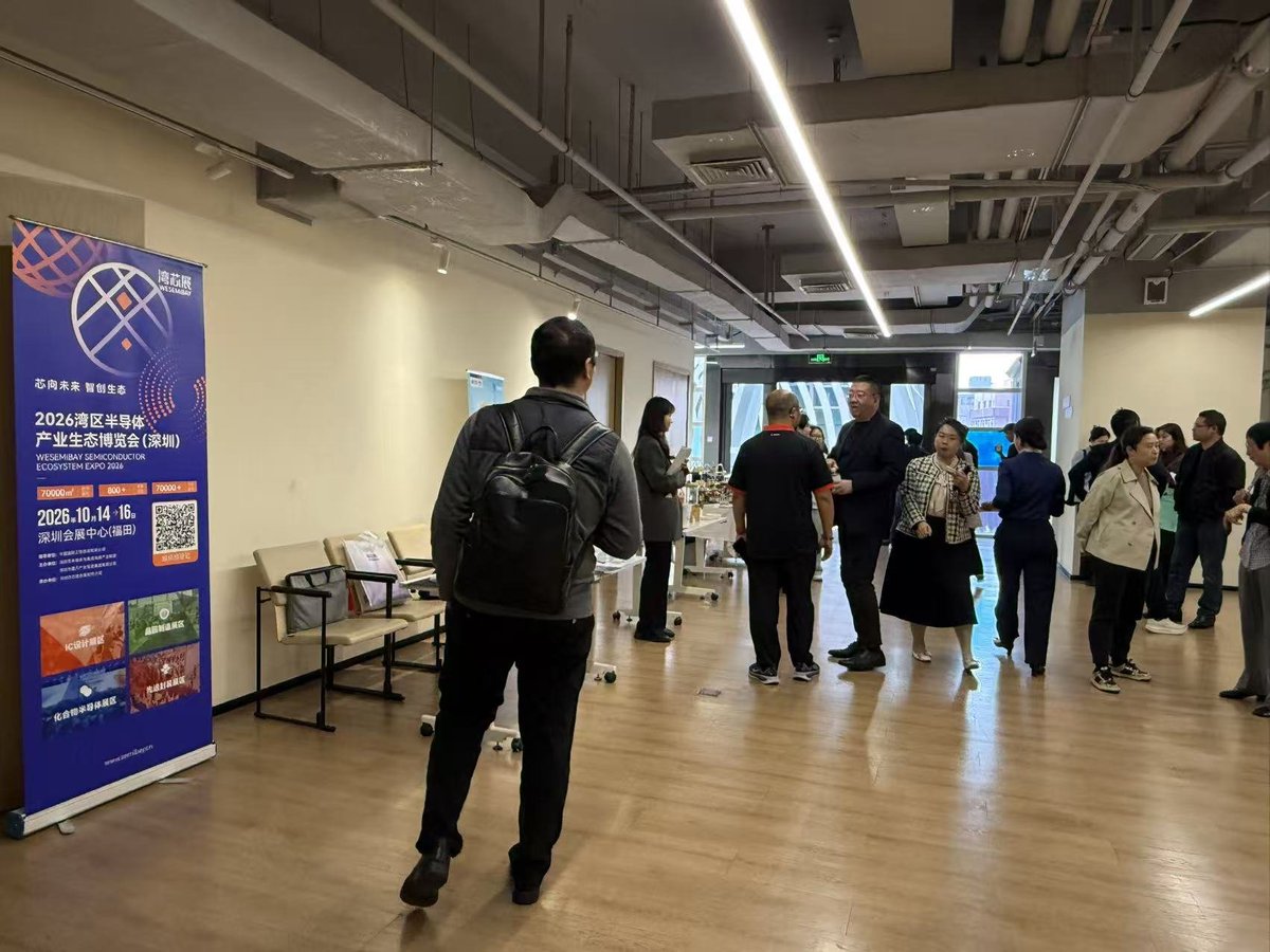
The event shared cutting-edge insights on advanced packaging, SiC power devices, equipment innovation and thermal management, empowering the semiconductor innovation and high-quality development. #China#SiC#Shenzhen#WESEMiBAY
Yuexin Semiconductor launches a $3.65 billion expansion project in Guangzhou, adding 40,000 12-inch wafers per month. As many high-end semiconductor tools rely on imports, this will create new orders for foreign equipment suppliers. #China#Wafer#WESEMiBAY
The WESEMiBAY Salon gathered 100+ engineers to explore RISC-V + AI for Embodied Intelligence, sharing deep insights with harmonious on-site discussions. #China#WESEMiBAY#RISC-V #AI#Robotics
Sanan & ST's Chongqing 8-inch SiC fab online! $3.2B invested, 480k wafers/year, mass production in Q4 2025. China's first automotive SiC line, partnering with top automakers for EV needs. #China#semiconductor#SiC
WESEMiBAY 2026 focuses on four zone: wafer fabrication, advanced packaging, compound semiconductor and IC design. Covering the semiconductor industry chain, we gather global resources, cutting-edge tech and opportunities for partners.#China#semiconductor#WESEMiBAY
WESEMiBAY is sponsored by the Shenzhen Semiconductor and Integrated Circuit Industry Alliance (SICA) and fully leveraging the vast application market in Shenzhen and the Greater Bay Area. #Exhibition#Semiconductor#WESEMiBAY