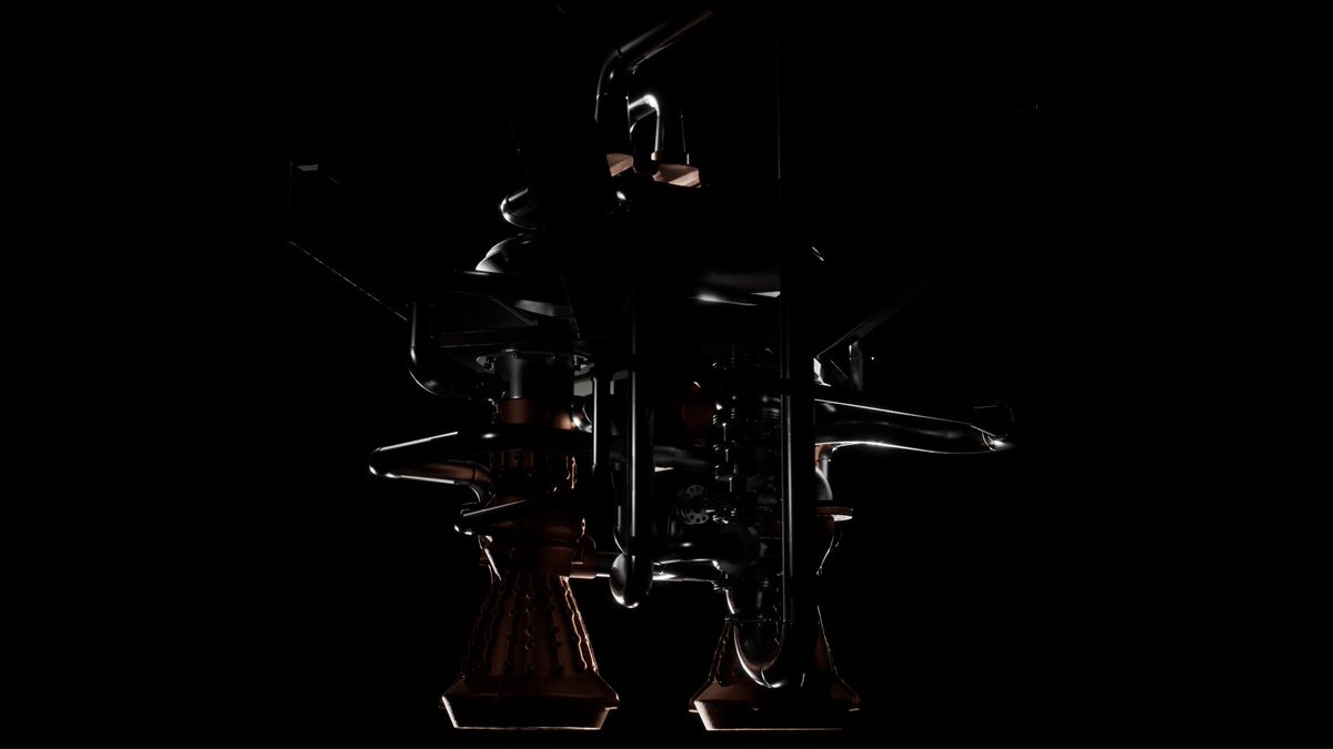
@theguildworld Why not choose LOX + Methane? It is cleaner for the engine. Using semi-cryogenic (RP-1/LOX class) propellants does not make an engine long-lasting.
A Dual Thrust Chamber 80kN engine, that will be breathed into life by our own Full-flow Segregated Cooling Cycle (FSCC). Historic. Pegasus, you beauty.
FSCC? 28.08.2026
Let’s see if @Grok 5 can beat the best human team @LeagueOfLegends in 2026 with these important constraints:
1. Can only look at the monitor with a camera, seeing no more than what a person with 20/20 vision would see.
2. Reaction latency and click rate no faster than human.
Join @xAI if you are interested in solving this element of AGI.
Note, Grok 5 is designed to be able to play any game just by reading the instructions and experimenting.
High-NA EUV timing is not a given.
This is Canon’s Inkjet Adaptive Planarization (IAP) high-volume manufacturing tool design, which they plan to begin shipping next year. The tool is likely essential to enable High-NA EUV lithography because of the technology’s limited depth of focus, a consequence of the larger lens size.
While Canon has addressed the throughput limitations of their prototype, what remains missing—in my view—is robust defect mitigation for the superflat wafer.
You can see the process flow for the modules inside this tool on the right. In the spreading module, a superflat wafer (manufactured by Shin-Etsu) presses the organic inkjetted planarization material into an extremely flat surface. The flatness data is impressive; it looks excellent and clearly solves the depth-of-focus challenge associated with High-NA.
However, Intel shared extensive defect data from the prototype tool, and it is clear that the superflat wafer poses a major production risk. The IAP process is far more sensitive to incoming particles on the wafer than CMP or virtually any other process tool. A single particle on one wafer in a lot tends to become embedded in the superflat and is then stamped onto every subsequent wafer. A repeating defect mode of this kind is a deal-breaker for a fab.
What I believe is still missing from this tool is comprehensive defect-containment processing for the superflat:
1) Inline metrology to detect any issues with the superflat in real time. One could envision a dual-stage system in which one superflat continues processing while its partner is measured to confirm it remains clean.
2) Automatic superflat swapping whenever a defect is detected by the system above. Having to manually take the tool down each time a defect appears in order to replace a compromised superflat would also be a deal-breaker. Ideally, finding a defect, swapping in a clean superflat, and continuing production should simply be business as usual.
Intel’s February presentation remains the best analysis to date of this tool’s production readiness, and—as noted—the defect modes associated with the superflat were identified as the primary barrier. One additional aspect that still needs to be addressed is post-processing of the IAP layer before photoresist coating.
Inspection metrology will definitely be required after a lot is processed to ensure there are no defects or planarization issues. This could involve multiple tools and add substantially to the process costs of High-NA EUV. Second, if any issue is found, the IAP layer will need to be reworked in the same way photoresist is reworked—again adding significant tooling and process cost.
The production readiness of this tool is only one factor affecting the High-NA EUV adoption timeline. Process cost is the other: as outlined above, IAP will introduce considerable tool and process costs that low-NA multipatterning simply does not have to contend with.