

Top Tweets for #Physicaldesign

Really excited for this journey. Feels surreal that conversations we’ve been having for years are now turning into a company.
Thanks @join_ef , @suhasasumukh , @localhostIND for all the support !!
Time to build @archgen_
#semiconductors #EDA #physicaldesign #ASIC #chipdesign #AI #chips

Thrilled to announce that @naveen_venk and I have joined @join_ef to build @archgen_ .
Our thesis is simple:
The next generation of semiconductor design tools will not just automate workflows they will learn from every engineer who uses them.
Chip design today is full of repeated manual effort.
1. A senior physical design engineer fixes a timing issue.
2. Another engineer solves a congestion problem.
3. Someone else discovers a better macro placement strategy.
4. A team spends weeks tuning PPA across hundreds of experiments.
But most of this knowledge disappears into scripts, logs, webex threads, reports, and individual engineer's memory.
We’re changing that.
At @archgen_ , we’re building self-learning agents for semiconductor design, with specific focus on physical design.
Our agents work alongside engineers, run EDA flows, inspect reports, debug failures, optimize PPA, and capture the reasoning behind successful workflows.
1. When an engineer solves something, the agent learns.
2. When a strategy fails, the agent remembers why.
3. When a similar problem appears again, the agent can reuse the right approach.
Over time, this becomes an organisational memory layer for chip design. One that compounds.
Our vision is to make chip design feel less like manually stitching together fragmented tools and more like working with a team of expert agents that get better every day.
The future of semiconductor design is self-learning.
Huge thanks to @suhasasumukh 🐐 and @localhosthq for being extremely generous with their credits and supporting us throughout.
#semiconductors #EDA #physicaldesign #ASIC #chipdesign #AI


Even With AI Inroads, Human Chip Designers Still Essential https://t.co/eu1ajjkZEX
#semiEDA #analog #verification #AI #workforce #chiparchitecture #physicaldesign #semiconductor


It's about understanding how people seek, use, and understand information – whether that information is a digital file or the location of the sugar...
#InformationArchitecture #DesignThinking #UserExperience #PhysicalDesign #Innovation #UXDesign
https://t.co/DnKac85Sh3

We’re Hiring – Physical Design Engineer
Looking for experienced professionals to join our VLSI team in Bangalore.
#WeAreHiring #PhysicalDesign #VLSIJobs #BangaloreJobs #HiringNow #ChipDesign #SemiconductorJobs #Innovus #FusionCompiler #ASICDesign #TechHiring #Speraspect


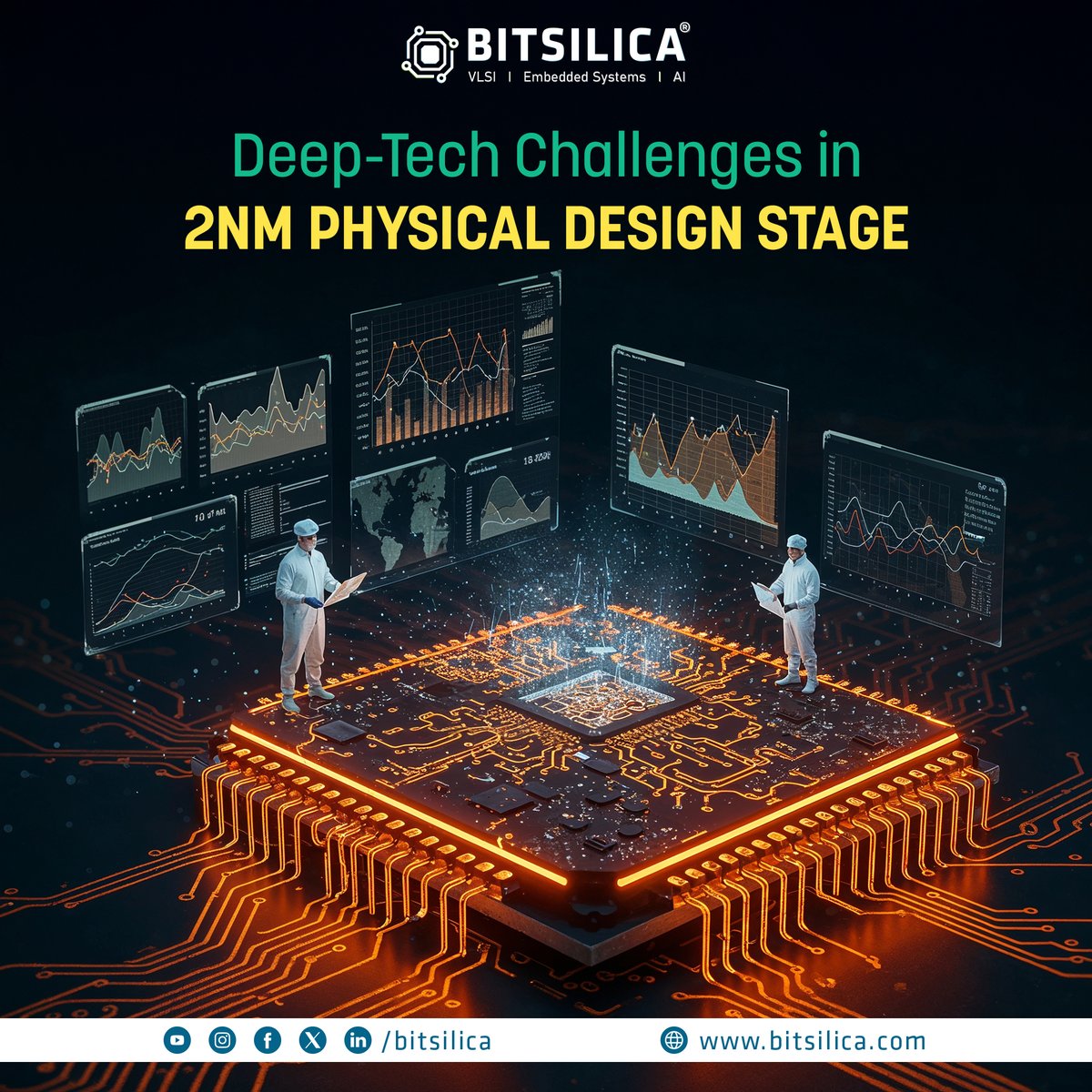
Designing at 2nm isn't just hard—it's quantum.
Challenges:
• Quantum tunneling
• Advanced DRCs
• PPA balancing
• Tool complexity
See how deep tech teams are solving the unsolvable:
🔗 https://t.co/9yNOplm76d
#2nm #Semiconductors #PhysicalDesign #EDA #ASIC #BITSILICA

🚀 Hiring Physical Design Engineers!
📍 Bangalore/Hyderabad
✅ 4–15 yrs exp | AMD flow, PNR, STA
⏳ Notice: 0–30 days
📩 [email protected]
#Hiring #PhysicalDesign #Jobs


Speeding Up Physical Design Verification for AMS Designs https://t.co/ia0Prv1B7g #Ams #CadenceVirtuoso #CalibrePatternMatching #CalibreRealtime #DesignSymmetry #PhysicalDesign

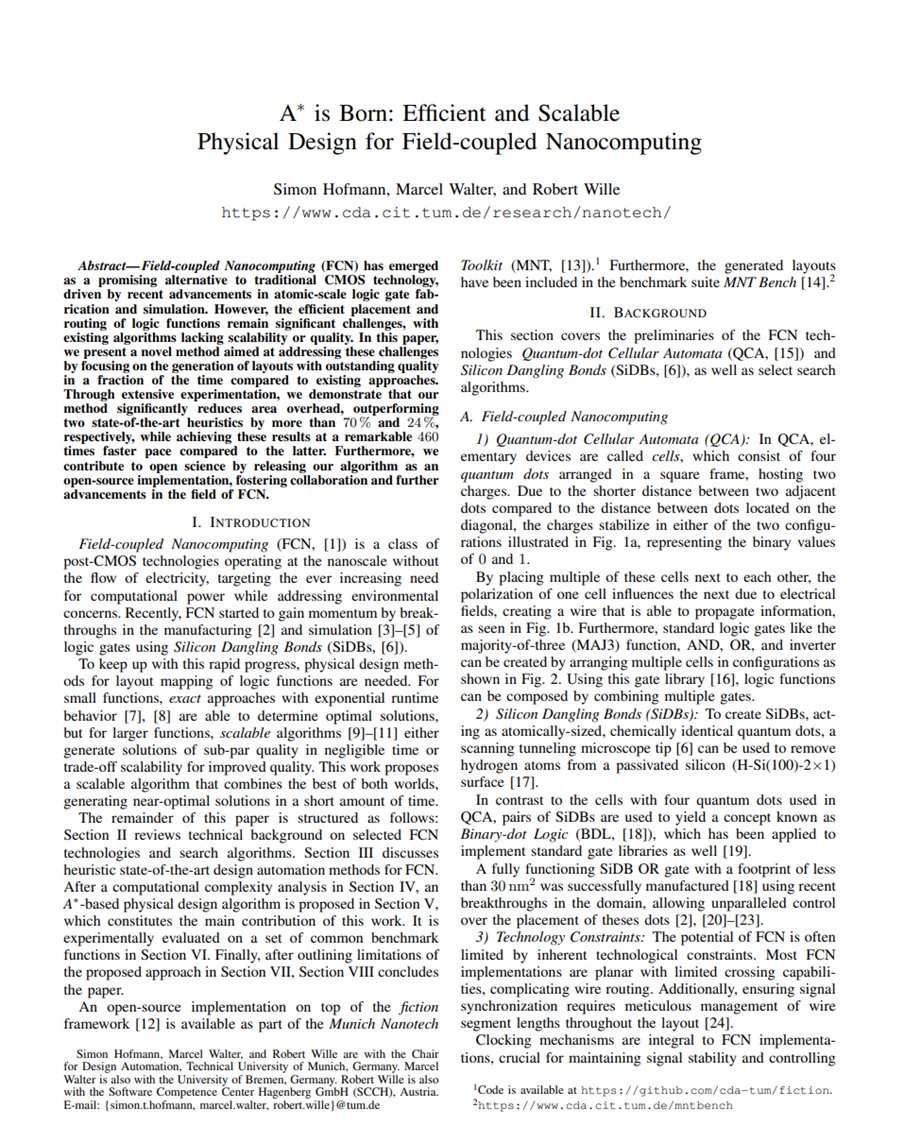
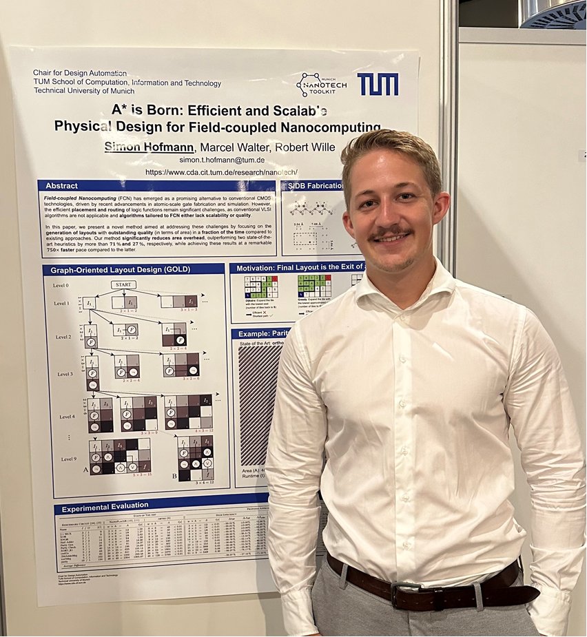
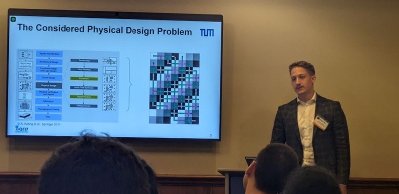
A* is born! And his name is Simon Hofmann!😅 Seriously, A* obviously is a powerful method that has been very successfully used in #DesignAutomation in the past. Today at @IEEENANO_Conf, Simon showed how to use this potential also for the #PhysicalDesign for #FCN.
1/2
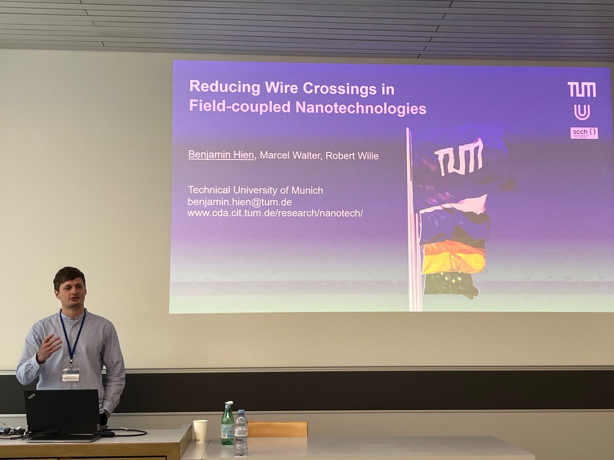
In Field-Coupled Nanotechnologies #FCN, wire crossings are the reason for substantial costs. Accordingly, new #PhysicalDesign methods considering that are needed. Ideas how they could look like were proposed this week by Benjamin Hien and @MarcelCavani at the #IWLS workshop.
Clocking constraints dominate the #PhysicalDesign for Field-coupled #Nanocomputing; and frequently put serious challenges in front of us. Now, Simon Hofmann (in a joint work with @ServadeiLorenzo and @MarcelCavani) came up with a brilliant idea: Think outside the clock!😉
1/2
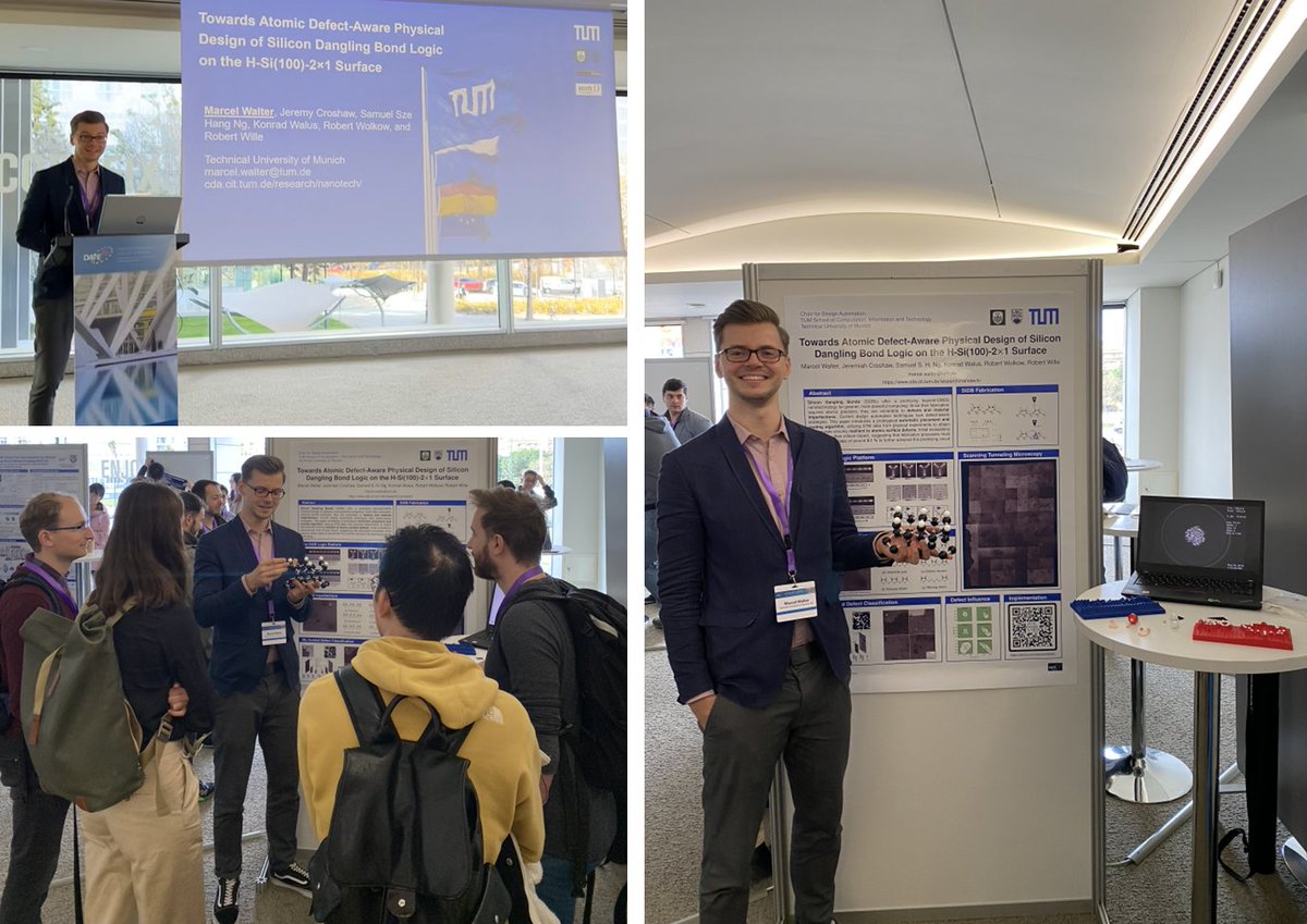
A #PhysicalDesign method for #Nanotechnologies (in particular #SiliconDanglingBonds) that explicitely takes experimentally verified defects into account! @MarcelCavani presented that today at @DateConference #DATE2024!🙂
1/2
We re-arranged our #DesignAutomation tools for nanotechnologies to realize different design flows, e.g., for #LogicSynthesis, #PhysicalDesign, and #Simulation. They are available in #opensource as part of the Munich Nanotech Toolkit.
Read more at
https://t.co/vzgg9H2XEe


よし!今日から本気出す!(あくまで他力本願)
試しに履いてみたら、ホントにお腹凹んだ🤣beforeがたるみすぎててafterとの差がすごくて宣伝広告みたい(笑)
#PHYSICALDESIGN
#トリプルエス
#お腹細見せガードル


Day 32: Law of Feedback (Part 2) 📢
Guiding actions!
This law isn't just for digital interactions. In physical spaces, clear signs direct users effortlessly. 🚶♀️
Ex: Gender based washroom Icons, use text to support & guide users!
#UXLaws #PhysicalDesign #DirectionalSigns

We believe what we see "Logic Synthesis and Static Timing Analysis (Uncut Version) currently at 50% discount
For more visit us at
For more courses Visit us at - https://t.co/2vim0e4FNt
#vlsiexpert #PhysicalDesign #Experience #PDEngineer #Physical DesignEngineer


Check out this video where Ranjit Jayprakash Yewale, Associate Director of Physical Design at Tessolve, takes us through the impressive physical design capabilities at Tessolve.
Watch the full video here: https://t.co/6Zs4quTb7x
#tessolve #physicaldesign #vlsi #chipdesign
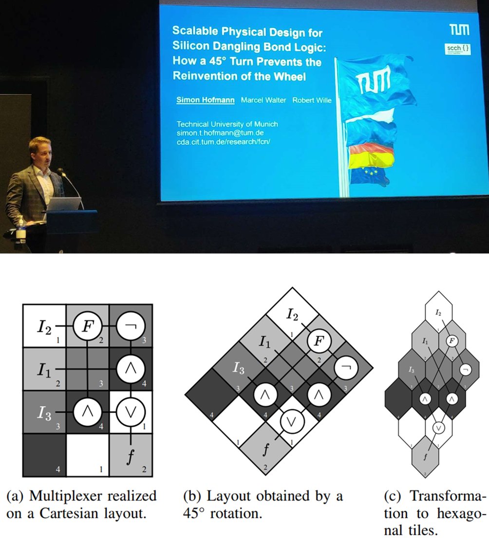
With a really neat idea (presented at IEEE #Nano today), Simon Hofmann saved us a lot of extra work in #PhysicalDesign for #SiDBs. He took approaches from #QCA and "turned them by 45°". The result: A top-notch SiDB design method that taps knowledge from decades of research!🙂
🚀 The Future of Physical Design is Here! 🌌
🔭 Explore the challenges and opportunities that await in the exciting realm of physical design. From complex integrated circuits to cutting-edge technologies, we're diving into the future of technology.
#SmartSoC #PhysicalDesign
Today, I had the pleasure to speak at the Int'l Symposium on Physical Design (#ISPD)---and to make the point that #PhysicalDesign expertise is exactly what we need for #QuantumCircuit mapping.
Our tool MQT QMAP provides a good starting point for this:
https://t.co/08jQYone9X


Hit 7K downloads today and counting. We humbly dedicate this milestone to Gorden Moore. @shivookoteshwar
#vlsi #soc #physicaldesign #moore https://t.co/6gEstkBTeb
Most Popular Users

Elon Musk 
@elonmusk
240.8M followers

Barack Obama
@barackobama
119.2M followers

Donald J. Trump
@realdonaldtrump
111.7M followers

Cristiano Ronaldo
@cristiano
111.3M followers

Narendra Modi
@narendramodi
107M followers

Rihanna
@rihanna
97.8M followers

NASA
@nasa
92.2M followers

Justin Bieber
@justinbieber
91.1M followers

KATY PERRY
@katyperry
88.1M followers

Taylor Swift
@taylorswift13
81.9M followers

Lady Gaga
@ladygaga
73.4M followers

Virat Kohli
@imvkohli
70.5M followers

Kim Kardashian
@kimkardashian
70M followers

YouTube
@youtube
68.7M followers

Bill Gates
@billgates
64.1M followers

Neymar Jr
@neymarjr
63.3M followers

The Ellen Show
@theellenshow
62.4M followers

CNN
@cnn
61.9M followers

Selena Gomez
@selenagomez
61.1M followers

X
@x
60.8M followers