

Top Tweets for #SeMes


#SEMES #Enfermería #Urgencias #Emergencias #Sanidad #EnfermeríaDeUrgencias #Salud #SistemaSanitario #SeguridadDelPaciente #EspecialidadesEnfermeras @SEMES_
Urgencias y UCI, en el centro del debate: SEMES reclama una especialidad propia de Enfermería
https://t.co/riKfRvCT3l


💛 Hoy, #DiaMundialPrevencionSuicidio, recordamos que prevenir también es escuchar, comprender, acompañar y pedir ayuda. Con el GdT de Salud Mental de SEMES
Reconocer las señales puede marcar la diferencia
📞 024 🚨 Emergencias: 112
No estás solo
#PrevenciónDelSuicidio #SEMES


oyşev in the 80s 🤎✨




Jornada Nacional de SEMES para TES 🚑
26 de octubre en Madrid
Os esperamos a tod@s!!!
#SEMES #TES #jornadanacional

🚑 Jornada Nacional de SEMES para Técnicos en Emergencias Sanitarias
#ConTEStos2026
📍Ministerio de Sanidad
🗓️ 26 octubre 2026. 10:30 h a 18:30 h.
Inscripciones: Gratuitas.
https://t.co/flgGP65MnC


Samsung Electronics Begins Construction of Hybrid Bonding Mass-Production Line at Pyeongtaek P5
Samsung Electronics has begun constructing a die-to-wafer (D2W) hybrid bonding mass-production line at its Pyeongtaek Campus. The line will be used to manufacture next-generation high-bandwidth memory (HBM) and logic semiconductors.
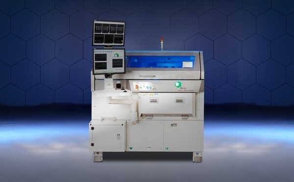
According to semiconductor industry sources on the 21st, Samsung Electronics has selected Dutch semiconductor back-end equipment maker BE Semiconductor Industries (Besi) as its preferred supplier and initiated the process of acquiring 50 D2W hybrid bonding machines. The equipment is slated for installation at the P5 fab on its Pyeongtaek Campus.
During Besi’s first-quarter earnings conference call in April, CEO Richard Blickman said, “We expect to see something more definitive regarding Samsung Electronics’ adoption of hybrid bonders around the middle of this year.” At the time, Besi’s hybrid bonders were undergoing Samsung’s qualification testing.
However, it will take more time to finalize the order. Samsung has requested modifications to the equipment architecture, making it difficult to determine a specific delivery date. Such modifications involve changing certain specifications—such as the design, components, or modules—to meet a customer’s requirements. The fact that Besi’s hybrid bonders cost approximately KRW 6 billion (about $4.3 million) each, roughly twice the price of competing products, is also said to be prolonging negotiations.
“Besi supplies hybrid bonders to semiconductor companies worldwide, including TSMC and Micron, and is reluctant to modify the equipment architecture exclusively for Samsung,” an industry source said. “Samsung considers Besi’s equipment the best option, but because coordination has been difficult, it is also considering products from Korean equipment makers that can respond more quickly and flexibly.”
SEMES, Samsung Electronics’ semiconductor equipment subsidiary, has also received a request to supply D2W hybrid bonders for the mass-production line. The company hopes to secure orders for two hybrid bonding production lines at the Pyeongtaek Campus.
“SEMES felt a strong sense of crisis when Samsung initially selected Besi’s equipment, but the situation has recently begun to change,” another industry source said.
SEMES completed development of its D2W hybrid bonder early this year and supplied a unit to Samsung Electronics for performance qualification. This suggests that the equipment has passed the testing process.
Samsung is also considering Hanwha Semitech as a hybrid bonder supplier. In February, Hanwha Semitech completed development of its second-generation D2W hybrid bonder, the “SHB2 Nano.” It subsequently supplied an evaluation unit to SK hynix in April.
The equipment was delivered as an integrated cluster system combining the bonder with a wafer-handling equipment front-end module (EFEM) from Cymechs, a plasma activation module from Hanwha Semitech, and a cleaning module from ZEUS.
Samsung’s construction of a D2W hybrid bonding mass-production line at its Pyeongtaek Campus is related to the packaging processes for HBM and logic semiconductors. According to industry sources, Samsung has pursued a hybrid bonding line for next-generation HBM at its Pyeongtaek Campus in addition to its Cheonan Campus, which serves as a major semiconductor back-end packaging hub.
Using hybrid copper bonding (HCB), rather than conventional thermocompression (TC) bonding, to stack HBM core dies (DRAM chips) can significantly improve performance, power consumption, and thermal characteristics. This is because the technology directly bonds copper and dielectric materials without using metal protrusions known as micro-bumps, thereby shortening the interconnect length between devices.
The technology is particularly likely to be used for customer-specific, or custom, HBM (cHBM). In cHBM, Samsung replaces the conventional base die with a logic die incorporating the customer’s computing circuitry and intellectual property (IP). This logic die assists external central processing units (CPUs) and graphics processing units (GPUs) with computation while optimizing data transmission.
Samsung plans to implement a three-dimensional system-in-package (3D SiP) architecture in which HBM DRAM layers are stacked vertically and directly on top of the logic die.
Samsung Electronics’ foundry business also unveiled “3D Cube-H,” a next-generation 3D vertical stacking solution based on hybrid bonding, last month. Designed for next-generation artificial intelligence chips and high-performance computing (HPC) systems, the heterogeneous integration packaging technology offers improved performance, power efficiency, and bandwidth compared with conventional packaging technologies. Samsung Foundry is currently actively proposing the solution to customers for adoption.
Hybrid bonders from the equipment suppliers are expected to begin arriving and being installed at the Pyeongtaek Campus toward the end of this year. However, Samsung internally expects large-scale production using hybrid bonding to become feasible around 2030, as the technology is considerably more challenging than TC bonding.
“We expect hybrid bonding to enter full-scale use around 2029, when Nvidia’s next-generation AI accelerator, Feynman, is expected to arrive,” a third industry source said.

El #ahogamiento es un problema de salud pública que mata a 400 personas cada año en España. El equipo #guardavidaskids te da unos consejos muy útiles para prevenirlo. Ojo a estos pequeños! #fundacionmapfre #semes @SemesSocorrismo
En #SEMES estamos de enhorabuena, y muy orgullosos!🤍
El Dr. Tato Vázquez Lima entre los mejores médicos del 2026 @elconfidencial
Gracias, presidente🤍💙
https://t.co/WH2kqYDBJQ


Semiconductor procurement strategies rarely rely on a single supplier due to the substantial upfront capital investment and costs involved. Currently, #BESI and #ASMPT lead the #D2W bonding equipment market. However, given the close relationship between #SEMES and #Samsung, #TrendForce expects that once SEMES achieves comparable technology maturity and production yields, it will gradually overtake BESI within Samsung's supply chain, mirroring the supplier transition previously seen in the TC bonding segment.
Samsung Electronics Begins Construction of Hybrid Bonding Mass-Production Line at Pyeongtaek P5
Samsung Electronics has begun constructing a die-to-wafer (D2W) hybrid bonding mass-production line at its Pyeongtaek Campus. The line will be used to manufacture next-generation high-bandwidth memory (HBM) and logic semiconductors.
According to semiconductor industry sources on the 21st, Samsung Electronics has selected Dutch semiconductor back-end equipment maker BE Semiconductor Industries (Besi) as its preferred supplier and initiated the process of acquiring 50 D2W hybrid bonding machines. The equipment is slated for installation at the P5 fab on its Pyeongtaek Campus.
During Besi’s first-quarter earnings conference call in April, CEO Richard Blickman said, “We expect to see something more definitive regarding Samsung Electronics’ adoption of hybrid bonders around the middle of this year.” At the time, Besi’s hybrid bonders were undergoing Samsung’s qualification testing.
However, it will take more time to finalize the order. Samsung has requested modifications to the equipment architecture, making it difficult to determine a specific delivery date. Such modifications involve changing certain specifications—such as the design, components, or modules—to meet a customer’s requirements. The fact that Besi’s hybrid bonders cost approximately KRW 6 billion (about $4.3 million) each, roughly twice the price of competing products, is also said to be prolonging negotiations.
“Besi supplies hybrid bonders to semiconductor companies worldwide, including TSMC and Micron, and is reluctant to modify the equipment architecture exclusively for Samsung,” an industry source said. “Samsung considers Besi’s equipment the best option, but because coordination has been difficult, it is also considering products from Korean equipment makers that can respond more quickly and flexibly.”
SEMES, Samsung Electronics’ semiconductor equipment subsidiary, has also received a request to supply D2W hybrid bonders for the mass-production line. The company hopes to secure orders for two hybrid bonding production lines at the Pyeongtaek Campus.
“SEMES felt a strong sense of crisis when Samsung initially selected Besi’s equipment, but the situation has recently begun to change,” another industry source said.
SEMES completed development of its D2W hybrid bonder early this year and supplied a unit to Samsung Electronics for performance qualification. This suggests that the equipment has passed the testing process.
Samsung is also considering Hanwha Semitech as a hybrid bonder supplier. In February, Hanwha Semitech completed development of its second-generation D2W hybrid bonder, the “SHB2 Nano.” It subsequently supplied an evaluation unit to SK hynix in April.
The equipment was delivered as an integrated cluster system combining the bonder with a wafer-handling equipment front-end module (EFEM) from Cymechs, a plasma activation module from Hanwha Semitech, and a cleaning module from ZEUS.
Samsung’s construction of a D2W hybrid bonding mass-production line at its Pyeongtaek Campus is related to the packaging processes for HBM and logic semiconductors. According to industry sources, Samsung has pursued a hybrid bonding line for next-generation HBM at its Pyeongtaek Campus in addition to its Cheonan Campus, which serves as a major semiconductor back-end packaging hub.
Using hybrid copper bonding (HCB), rather than conventional thermocompression (TC) bonding, to stack HBM core dies (DRAM chips) can significantly improve performance, power consumption, and thermal characteristics. This is because the technology directly bonds copper and dielectric materials without using metal protrusions known as micro-bumps, thereby shortening the interconnect length between devices.
The technology is particularly likely to be used for customer-specific, or custom, HBM (cHBM). In cHBM, Samsung replaces the conventional base die with a logic die incorporating the customer’s computing circuitry and intellectual property (IP). This logic die assists external central processing units (CPUs) and graphics processing units (GPUs) with computation while optimizing data transmission.
Samsung plans to implement a three-dimensional system-in-package (3D SiP) architecture in which HBM DRAM layers are stacked vertically and directly on top of the logic die.
Samsung Electronics’ foundry business also unveiled “3D Cube-H,” a next-generation 3D vertical stacking solution based on hybrid bonding, last month. Designed for next-generation artificial intelligence chips and high-performance computing (HPC) systems, the heterogeneous integration packaging technology offers improved performance, power efficiency, and bandwidth compared with conventional packaging technologies. Samsung Foundry is currently actively proposing the solution to customers for adoption.
Hybrid bonders from the equipment suppliers are expected to begin arriving and being installed at the Pyeongtaek Campus toward the end of this year. However, Samsung internally expects large-scale production using hybrid bonding to become feasible around 2030, as the technology is considerably more challenging than TC bonding.
“We expect hybrid bonding to enter full-scale use around 2029, when Nvidia’s next-generation AI accelerator, Feynman, is expected to arrive,” a third industry source said.
🚑 Reservaos el 26 de octubre de 2026…
#TES
#TécnicosEmergenciasSanitarias
#ConTEStos2026
#SEMES
@SEMES_


la investigación en Urgencias y Emergencias.
🔗Más info en nuestra web: https://t.co/b5m91H4r2X
@SEMES_
#SEMES #SEMESAndalucíaUrgencias


👩⚕️👨⚕️🚑 Durante los días 16 y 17 de junio se ha celebrado con gran éxito el Curso de Soporte Vital Pediátrico con certificación ERC (EPALS), organizado por SEMES Andalucía.
Gracias a todos los asistentes💙
#SEMES #SEMESAndalucíaUrgencias


Hola! Hoy, las aventuras de Sophie, La Enfermera, ¡llegan a Zaragoza!
#Zaragoza #laenfermera #novela #novedad #urgencias #semes #enfermería

🏥📚 Urgencias del Hospital Universitario de Jerez participa en el 36º Congreso Nacional de #SEMES con varios trabajos científicos, entre ellos el póster "Enfermería Finalista en Urgencias II: Suturas".
#SomosAreaJerezCostaSierra

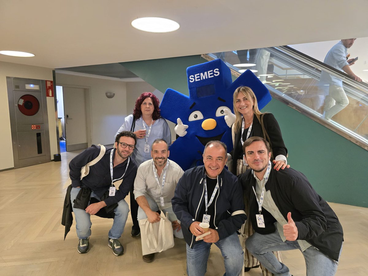


Seguimos con la segunda charla !!
Raro .. de urgencias a UCI !#semes

Estamos en Semes … trabajando para enfermedades raras !#semes
La Dra Lopez de Lugo … nos cuenta cómo enfrentarnos a ellas

Desde SEMES Sanidad Táctica lamentamos profundamente la pérdida de nuestro compañero MINTXO, miembro de Policía Foral de Navarra, fallecido en accidente de tráfico.
Servicio, compromiso y compañerismo hasta el final.
Descansa en paz, compañero. 🖤
#DEP #PoliciaForal #SEMES


Finalizó el día del “Emergency Medicine Day” con el encendido de edificios emblemáticos de la provincia 🏛️💡
#SEMES #SEMESAndalucíaUrgencias




Last Seen Hashtags on Sotwe
elpurpura
Seen from United States
JungKookIAmStillPartyAtSMCinema
Seen from United States
MonsoonSkinIssues
Seen from United States
mlm
Seen from United States
معصيتي_رحتيي
Seen from Spain
zoosarevalid
Seen from United Kingdom
Ideas2Action
Seen from United States
computerfreetips
Seen from United States
cuckold #wife #porn
Seen from Netherlands
publicsex #asian
Seen from Germany
Trends for you
Most Popular Users

Elon Musk 
@elonmusk
241.7M followers

Barack Obama
@barackobama
119M followers

Cristiano Ronaldo
@cristiano
114.4M followers

Donald J. Trump
@realdonaldtrump
111.9M followers

Narendra Modi
@narendramodi
107.2M followers

Rihanna
@rihanna
98.7M followers

NASA
@nasa
92.4M followers

Justin Bieber
@justinbieber
91.8M followers

KATY PERRY
@katyperry
90M followers

Taylor Swift
@taylorswift13
83.9M followers

Lady Gaga
@ladygaga
75.4M followers

Virat Kohli
@imvkohli
73.4M followers

Kim Kardashian
@kimkardashian
70.9M followers

YouTube
@youtube
68.8M followers

Neymar Jr
@neymarjr
66.4M followers

Bill Gates
@billgates
65.2M followers

Selena Gomez
@selenagomez
63.1M followers

The Ellen Show
@theellenshow
62.3M followers

CNN
@cnn
61.8M followers

X
@x
60.7M followers