

Top Tweets for #pcbdesigntools

Understanding Proper #PCB Design – Part 1
4-Layer Board Design
Printed circuit boards (PCBs) have become a fundamental staple at the heart of most ...CLICK TO READ MORE https://t.co/ByKX7SiIND #PCBrouting #PCBdesigntools #PCBDesign
Understanding Proper #PCB Design – Part 1
4-Layer Board Design
Printed circuit boards (PCBs) have become a fundamental staple at the heart of most ...CLICK TO READ MORE https://t.co/ByKX7SiIND #PCBrouting #PCBDesign #PCBdesigntools
Understanding Proper #PCB Design – Part 1
4-Layer Board Design
Printed circuit boards (PCBs) have become a fundamental staple at the heart of most ...CLICK TO READ MORE https://t.co/ByKX7SiIND #PCBrouting #PCBDesign #PCBdesigntools

Need some guidance on PCB design?
Download NCAB Group's checklist of PCB design guidelines below.
https://t.co/L5Y8KLnqci
#pcbdesign #pcbdesigntools #stackups #impedance #ncab #ncabgroup #electronicsweekly

Designing a Printed Circuit Board
Printed circuit boards (PCBs) make most of the electrical connections in modern electronics. A #PCB is an insulating material with copper glued to one ...CLICK TO READ MORE https://t.co/UfwWpDQgKS #PCBDesign #PCBdesigntools
Understanding Proper #PCB Design – Part 1
4-Layer Board Design
Printed circuit boards (PCBs) have become a fundamental staple at the heart of most electronic systems. ...CLICK TO READ MORE https://t.co/ByKX7SiIND #PCBdesigntools #PCBrouting #PCBDesign
Understanding Proper #PCB Design – Part 1
4-Layer Board Design
Printed circuit boards (PCBs) have become a fundamental staple at the heart of most electronic systems. ...CLICK TO READ MORE https://t.co/ByKX7SiIND #PCBDesign #PCBrouting #PCBdesigntools
Understanding Proper #PCB Design – Part 1
4-Layer Board Design
Printed circuit boards (PCBs) have become a fundamental staple at the heart of most electronic systems. ...CLICK TO READ MORE https://t.co/ByKX7SiIND #PCBDesign #PCBdesigntools #PCBrouting
The design-for-manufacturing (DFM) capabilities of today’s PCB design suites are getting more sophisticated, leveraging cloud-based collaboration and more. @altium @Cadence @siemenssoftware @ZukenAmericas #designformanufacturing #PCBdesigntools #PCBDFM
https://t.co/e2gI08epKc
In this series, Robert examines the important aspects that are critical to good PCB design. Here in Part 1, he shares the step-by-step method he uses to design four-layer PCBs. #proteus #labcenter @pentalogix @kicad_pcb #PCB #PCBDesign #PCBdesigntools
https://t.co/DKaDgHKrd3
In his July Circuit Cellar editorial, Chief Editor Jeff Child takes a look at how PCB design has evolved in his lifetime, recalling the days of PCB layout edits made using X-Acto knives and PCB verification using highlighter markers. #PCBdesigntools https://t.co/bNTHc4cWNn

Starting in just 30 minutes join ED and Jorge for Part 1 of Getting Started with EAGLE webinar November session! https://t.co/QYVGvYL7KD 10/12 @ 2PM EDT #diyelectronics #ECAD #PCBdesigntools #engineering

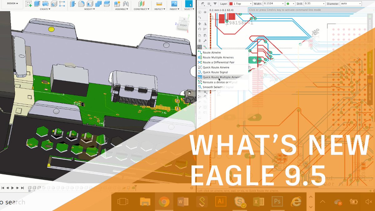
Watch the What's New in Autodesk EAGLE v9.5 recorded live session now on demand! See how Shared Managed Libraries, Persistent Groups, ReRoute Command can speed up your #PCBdesign workflow! https://t.co/REgDmT5Dy7
We're at #PCBWest2019 #PCBWest #PCBdesigntools
T-minus 16 hours until we turn on the reflow ovens and kick off the soldering station at the Autodesk EAGLE booth #101 at #PCBWest2019! https://t.co/kTSWW8BT4n
#PCBDesigntools for everyone! @adskeagle @PCBWest #PCBWest #PCBDesign
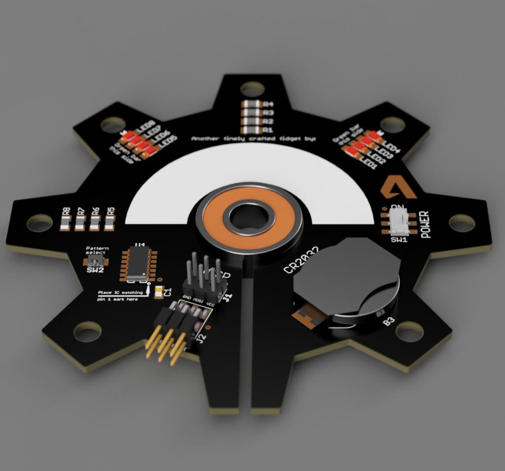
Who's ready for #PCBWEST2019!? Join the Autodesk EAGLE team @ Booth 101 on 9/10 to learn about the newest #PCBdesigntools and integrated ECAD/MCAD workflows with @adskFusion360! #SiliconValley #SantaClara #PCBdesign @PCBWest

New to #PCBdesign or Autodesk EAGLE? Then don't miss today's Getting Started with EAGLE class 9/3 @ 2PM EDT! https://t.co/yOaqmK7XSa
#PCBdesigntools #Autodesk

Join Ed and Jorge on 9/5 @ 2PM EDT to unwrap the newest tools just added in Autodesk EAGLE 9.5! Get a preview of the new Shared Libraries, Persistent Groups and more.
https://t.co/R8ZfTTTcMP #PCBdesigntools #PCBdesign

Project the surface of your @adskFusion360
designed enclosure to create the PCB outline in EAGLE. Learn how with the Quick Tip of the Day! https://t.co/FaaEP6hslk #ECAD #MCAD #PCBdesign #PCBdesigntools

Come meet the Autodesk EAGLE team in Santa Clara, CA on Sept 10th at @PCBWest! Get your tickets here https://t.co/OlMruhQtf1 #SiliconValley #PCBdesigntools #MakeAnything #PCBFab #PCBDesign #Engineering #PCBWest2019

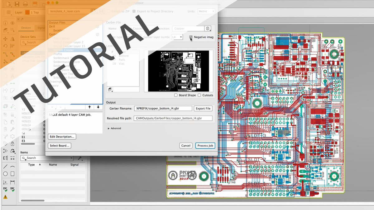
1-Click CAM Data Generation in EAGLE! Learn how to quickly get your board files ready for production at a board house in just under 4 min. https://t.co/v5B0HELXpx #PCBdesign #PCBdesigntools #MFG @ADSKEAGLE
Last Seen Hashtags on Sotwe
Most Popular Users

Elon Musk 
@elonmusk
241.5M followers

Barack Obama
@barackobama
118.8M followers

Cristiano Ronaldo
@cristiano
114.6M followers

Donald J. Trump
@realdonaldtrump
111.8M followers

Narendra Modi
@narendramodi
107.1M followers

Rihanna
@rihanna
98.7M followers

NASA
@nasa
92.3M followers

Justin Bieber
@justinbieber
91.8M followers

KATY PERRY
@katyperry
90M followers

Taylor Swift
@taylorswift13
84M followers

Lady Gaga
@ladygaga
75.5M followers

Virat Kohli
@imvkohli
73.5M followers

Kim Kardashian
@kimkardashian
70.9M followers

YouTube
@youtube
68.8M followers

Neymar Jr
@neymarjr
66.5M followers

Bill Gates
@billgates
65.3M followers

Selena Gomez
@selenagomez
63.1M followers

The Ellen Show
@theellenshow
62.2M followers

CNN
@cnn
61.7M followers

X
@x
60.7M followers