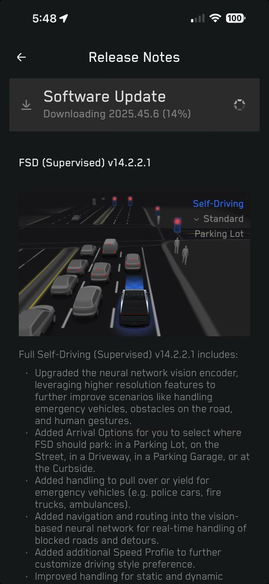
This 2020 Tesla Model Y Dual-Motor Long Range is even better than my Model 3. Like most Teslas, it almost drives itself. Extremely fun and almost free to drive with energy coming from the solar panels on my home.
It’s pretty wild how K.I.T.T. is basically a Tesla.
44 years later, Tesla vehicles drive themselves, think with advanced AI, and even come with an AI companion (Grok).
Watching this show reminds me that we are indeed living in the future.
GOOD NEWS 🚨 TESLA HAS REINVENTED THE MOSFET WITH THE "SIDE-SOURCE" ARCHITECTURE TO UNLOCK THE 48V ERA 🐳
Sometimes the biggest leaps in performance come from the smallest shifts in geometry. This philosophy is the driving force behind Tesla’s latest effort to reinvent the humble MOSFET package.
For those unfamiliar with the term, a MOSFET is simply a high-speed digital switch. Think of it as a gatekeeper that turns electricity on and off thousands of times per second to control how fast a motor spins or how bright a light shines. It is the fundamental building block of the "nervous system" for next-generation vehicles.
But this is not just a standard part. Recognizing its critical role in their future, Tesla has treated this hardware with a level of secrecy usually reserved for their most advanced software.
While the world focused on the arrival of the massive AI5 computer, Tesla quietly secured the blueprint for something arguably more foundational. In a move that signals a tactical blockade of the global supply chain, they chose to file this patent exclusively in Japan, South Korea, and China.
Patent JP 2025121890 A pulls back the curtain on this new, ultra-low-inductance chip design. It serves as the physical "muscle fiber" required to make Tesla's next-generation machines move.
This patent provides the first technical explanation for the breakthrough efficiency visible in the 2026 Cybercab fleet. The new self-driving computer is a power-hungry beast that consumes immense energy legacy 12V systems simply cannot deliver.
However, moving to a higher-voltage 48V standard to satisfy this hunger creates its own dangers. This is where the new chip becomes the linchpin.
It serves as the fundamental building block that makes the "unboxed" architecture viable at scale by neutralizing the electrical noise that typically plagues high-power systems. Without this specific component, the efficiency targets for the next generation of vehicles and robots would remain theoretical.
To understand why Tesla is betting its future on this tiny package, we first need to understand the invisible force it is designed to fight.
🚧 The problem: the invisible barrier of parasitic inductance
The core technical challenge addressed in this patent is the phenomenon of parasitic inductance during high-speed switching. In power electronics, such as the inverters that convert DC battery power to AC for the motor, transistors like MOSFETs must switch on and off thousands of times per second.
In traditional semiconductor packages, the physical distance between the source and drain terminals creates a large current loop. When current changes rapidly, this loop acts like an inductor. It resists the change and creates dangerous voltage spikes and "ringing" or oscillations.
These spikes can damage components, generate excessive heat, and force engineers to artificially limit switching speeds. This significantly reduces the overall efficiency and performance of the vehicle's powertrain.
To break through this barrier, Tesla could not just tweak the existing design. They had to dismantle the loop entirely.
📐 Tesla's solution: the "side source" snubber architecture
Tesla’s solution is a radical redesign of the semiconductor package's physical footprint to suffocate voltage spikes at the source. Think of these spikes like the loud "bang" or water hammer you hear in old plumbing when you turn off a faucet too quickly. This effect happens with electricity too and can damage the system.
Instead of relying on the traditional layout where source and drain terminals are solely on opposite ends of the chip, this design introduces "side source terminals".
These are positioned physically adjacent to the drain terminals on the package's lateral sides. This proximity is not accidental. It is calculated to allow for the connection of an external "snubber" capacitor directly bridging the source and drain with a minimal physical gap.
This capacitor acts like a shock absorber for the electrical circuit. By integrating these connection points directly into the lead frame architecture, the design shrinks the "commutation loop", which is simply the physical path the electricity travels, to a microscopic level.
This effectively absorbs the excess transient energy instantly and allows the device to run cooler and faster. However, running faster usually generates heat.
This required Tesla to rethink not just the electrical connections, but the thermal ones as well.
🧊 Thermal management: flipping the script on heat dissipation
The patent details a sophisticated top-side cooling architecture where the heat spreader, often called a clip or die paddle, is exposed on the top surface of the package rather than the bottom. This is similar to moving a building's heavy air conditioning units to the roof so the basement is free for plumbing and wiring.
This design choice is strategic because it frees up the bottom of the device, the side facing the printed circuit board, for complex electrical routing without being constrained by thermal interface materials.
By moving the primary cooling path to the top, Tesla can place the snubber capacitors and high-current traces on the PCB immediately beneath or alongside the chip. This minimizes the electrical path length and resistance to ensure that the cooling solution does not interfere with the critical goal of inductance reduction.
With the thermal constraints lifted, the design focuses on maximizing the geometric efficiency of the electrical path.
📉 Efficiency: the physics of the "triangular" loop
The document describes a specific geometric arrangement to combat signal distortion. When high-speed signals are applied, the layout of the Printed Circuit Board traces can inadvertently create inductive loops. These loops act like speed bumps that slow down the energy transfer.
Tesla's design utilizes the new side source leads to form a tight "triangular" loop area with the external capacitor. The patent data suggests that bridging the drain and source directly with this specific package geometry significantly reduces parasitic inductance compared to standard layouts.
This allows the MOSFETs to switch cleanly without the jagged voltage overshoots that typically plague high-power systems. Ultimately, this results in more battery energy making it to the wheels rather than being lost as waste heat. But raw efficiency is useless without control. This leads to the next critical innovation hidden inside the package.
🎯 Precision control: the Kelvin source integration
Hidden within the terminal layout is a subtle but game-changing feature mentioned in the patent claims called the "Kelvin Source" terminal. In high-power switching, the massive current flowing through the main source terminal creates a voltage drop that can confuse the gate driver. This is the component responsible for turning the switch on and off.
Imagine trying to hold a conversation in a crowded stadium where the noise drowns out your voice. The Kelvin source is like using a private phone line to talk instead. This patent separates the high-current path, representing the crowd, from the control signal path, representing the private line.
By including a dedicated Kelvin source pin that connects internally to the die but carries no load current, Tesla ensures the gate driver sees the true voltage of the source. This allows for incredibly precise switching timing. It shaves off nanoseconds of inefficiency that usually get lost in signal noise and further reduces heat generation.
Yet, all this delicate internal geometry must survive the brutal reality of the automotive environment.
🧱 Structural integrity: the notched lead frame
To accommodate these new side terminals without compromising the package's durability, the design features specific notches cut into the heat spreader around the side source terminals. These notches serve a dual function that aids both manufacturing and operation.
Electrically, they provide necessary clearance known as "creepage distance". This is used to prevent arcing. Arcing is when electricity jumps through the air like a miniature lightning bolt. This notch acts as a safety gap or firebreak to keep the high-voltage drain components safely away from the low-voltage source components.
Mechanically, the side terminals act as additional support points for the heat spreader. This ensures that during the high-pressure molding process and subsequent soldering, the internal components remain perfectly aligned. It prevents the warping or tilting that can lead to premature device failure in the harsh vibration environment of a vehicle.
This ruggedness allows individual chips to be packed densely together to form a larger system.
🧩 Scalability: the 180-degree array configuration
The patent extends beyond a single chip to describe how these packages function as a system. The symmetrical yet offset nature of the side terminals allows two packaged components to be mounted side-by-side but rotated 180 degrees relative to one another.
This "yin-yang" style configuration is like fitting Tetris blocks together perfectly and allows for extremely high packing density on the inverter board.
By rotating the devices, the drain terminals of one chip align near the source terminals of its neighbor. This allows them to potentially share capacitor banks or simplify the busbar routing. This density is vital for shrinking the overall size of the drive unit, which is a critical factor in next-generation vehicle architectures where space is at a premium.
And this universal footprint is designed to support not just today's silicon, but the materials of tomorrow.
🧪 Material agnosticism: ready for the GaN era
While the patent applies to standard Silicon MOSFETs, the text explicitly calls out "GaN MOSFETs" or Gallium Nitride as a primary candidate for this package. This is significant because GaN is an advanced material that acts like a high-performance sports car engine compared to the reliable sedan engine of standard silicon.
It switches faster but is notoriously sensitive to the parasitic inductance this patent aims to eliminate. Traditional packaging often bottlenecks GaN performance. However, this low-inductance "side-source" design appears specifically engineered to unleash the full potential of wide-bandgap materials.
This suggests Tesla is future-proofing their supply chain by creating a universal package footprint. It can host affordable Silicon chips today and swap to high-performance GaN chips tomorrow without redesigning the entire circuit board.
This adaptability is essential because these chips are destined for a specific and revolutionary electrical standard.
🔋 The 48V standard: redefining the "low voltage" grid
Perhaps the most telling detail in the document is the specified voltage range of "12V to 150V." This specific range strongly implies this technology is the backbone of Tesla’s transition to a 48V vehicle architecture debuted in the Cybertruck.
To understand why this matters, we need to look at the three different "blood pressures" of an electric car. First, there is the legacy 12V standard. For decades, cars used this low-pressure system for everything from radios to headlights. It is safe and cheap. However, like trying to water a garden with a drinking straw, it struggles to deliver high power without using thick and heavy copper wires.
Second, there is the 800V propulsion system. This is the massive "fire hose" pressure used only to spin the wheels and fast-charge the battery. It is efficient but dangerous to touch and overkill for small components.
Finally, there is the 48V standard. This is the new "sweet spot" where Tesla is moving all its auxiliary loads. These are the "accessories" that do not move the car, such as power steering motors, window regulators, air conditioning fans, and self-driving computers.
By moving these accessories to 48V, Tesla increases the electrical "pressure." This allows them to use much thinner and lighter wires to move the same amount of power, similar to how a high-pressure washer uses a thin hose to do the same work as a thick garden hose.
However, increasing the voltage creates new challenges. Power density increases, meaning more energy is crammed into smaller chips, which generates concentrated heat. Additionally, switching at higher voltages can create electromagnetic interference or electrical "noise" that acts like static on a radio and can confuse nearby sensors.
This patent appears to be the "workhorse" chip package designed to solve these exact problems. It handles the heat of 48V loads and suppresses the electrical noise. This ensures that the move to lighter and efficient wiring does not come at the cost of reliability.
And because this technology is so critical to Tesla's future, they have deployed a unique legal strategy to protect it.
🌏 Strategic deployment: why Japan, Korea, and China?
A distinct pattern emerges in the filing locations of Japan, Korea, and China. While these patents claim priority from a US Provisional application (63/550,927), that initial document remains unpublished by law and serves only as a secret placeholder.
Tesla’s decision to formally prosecute this technology in Asia before the US reveals a calculated urgency. They are less concerned with American copycats and focused entirely on locking down the Asian supply chain where the actual hardware is built.
These three nations form the "Iron Triangle" of semiconductor manufacturing. They host power giants like Toshiba in Japan, advanced fabrication in Korea, and the world's largest assembly market in China.
By prioritizing intellectual property rights here, Tesla is effectively patenting the recipe inside the competitor's kitchen. This legal blockade prevents local manufacturers from producing this specific low-inductance design for rivals. It ensures that if a factory in Shenzhen or Kyoto builds this chip, they can only sell it to Tesla.
The strategy protects against a "commodity trap" where unique engineering becomes a generic standard. While the internal silicon MOSFETs are common components, the "secret sauce" lies in the proprietary package geometry and cooling interface.
Without these specific protections, generic chipmakers could clone the physical design to sell "Tesla-compatible" high-efficiency parts to competitors. These filings create a robust firewall and guarantee that the efficiency advantages of this architecture remain exclusive to Tesla's ecosystem.
Ultimately, this protection is vital because this chip is not just a component. It is the foundation for Tesla's most ambitious products.
🤖 How this patent contributes to Tesla's now and future
This patent serves as the hardware backbone for Tesla's two most ambitious pillars. These are the autonomous "Cybercab" fleet and the Optimus humanoid robot. It confirms that Tesla is standardizing a single and robust 48V power architecture across its entire product ecosystem, from four-wheeled robotaxis to two-legged androids.
For the Cybercab, this low-inductance package is the key enabler for the "Unboxed" manufacturing process. By handling the higher power densities of a 48V zonal system with zero wasted heat, it allows the vehicle to shed heavy 12V wiring harnesses and reduces copper use by up to 70%. This rugged design ensures the fleet can operate on nearly 24/7 duty cycles with the reliability required for a driverless service.
For Optimus, this chip acts as the robot's "nervous system." It utilizes the patent's "Kelvin Source" feature to unlock human-like dexterity. To perform delicate tasks like folding laundry or handling fragile objects, the robot requires ultra-precise torque control. By isolating control signals from electrical noise, this chip ensures the motors receive clean and accurate commands. This gives Optimus the fine motor skills necessary for general-purpose work.
Furthermore, the top-side cooling architecture solves the critical space constraints of a humanoid form factor. Unlike a car with ample space, a robot must pack dozens of actuators into human-sized limbs. This design allows matchbox-sized inverters to be pressed directly against the robot’s structural metal skeleton for heat dissipation. This enables Optimus to hold heavy static loads without overheating its enclosed actuators.
Ultimately, this patent proves that Tesla is not just building a car part. They have created a universal "muscle controller" that will drive the movement of every machine they build in the AI era.
@money_cruncher In 2008 I bought a like new condition 2005 Toyota Sienna w/ 51,000 miles for 50% of the new one on the sfowroom floor..
The depreciation on the Tesla is normal - not outrageous !!!
@eternlwallet The Android version of V2 needs to be fixed. The Android 15 system drawer overlays the bottom of the V2 screens making the bottom of the V2 screens unusable. The screens need to be shortened so the bottom of the screens can be usable for navigating to other screens.
So let me get this straight, Elon is implanting products from Neuralink into humans to help people that have lost the use of their limbs, accelerating the world’s transition to sustainable energy to save earth with Tesla while creating a humanoid robot that will essentially be able to do anything, launching Starlinks every week to space orbit to connect the world to the best internet while building out Starship to save human consciousness by making life multi-planetary, fighting soul sucking traffic by digging Boring Tunnels underneath the ground, and building an “everything” app that is fundamentally fighting for the freedom of speech & the truth…
And you hate this guy?
WTF is wrong with you people. I would like to know what you did this past week.
! ! ! ! B R E A K I N G ! ! !
Welcome Tesla to use 48V low voltage system!
-1955 = 6V system
1955-2023 = 12V system
(24V on heavy trucks)
2023, Tesla, 48V system
Tesla just sent out a pdf to all car manufacturer telling them how to make a 48V system.
When will they adapt 48V as they did with NACS?
The list of companies joined 48V are:
❌ Aptera
❌ Ford
❌ GM
❌ Rivian
❌ Volvo
❌ Polestar
❌ Mercedes
❌ Nissan
❌ Fisker
❌ Honda
❌ Jaguar
❌ Hyundai
❌ Kia
❌ BMW
❌ Toyota
❌ Subaru
❌ Lucid
❌ Stellantis
❌ Volkswagen group
BREAKING: In a devastating speech, iconic actor Robert De Niro rips Donald Trump to shreds, declaring that Trump is “not a bad man,” but “an evil one” who is a “wanna be tough guy” and has “no morals or ethics.”
But Robert De Niro didn’t stop there…
De Niro continued:
“Trump has no sense of right or wrong. No regard for anyone but himself — not the people he was supposed to lead and protect, not the people he does business with, not the people who follow him, blindly and loyally, not even the people who consider themselves his “friends.” He has contempt for all of them.
The repercussions of his turbulent presidency divided America and rattled New York City beyond imagination. Remember how we were jolted by crisis in early 2020, as a virus swept the world.
We lived with Donald Trump’s bombastic behavior every day on the national stage, and we suffered as we saw our neighbors piling up in body bags.
The man who was supposed to protect this country put it in peril, because of his recklessness and impulsiveness. It was like an abusive father ruling the family by fear and violent behavior. That was the consequence of New York’s warning getting ignored. Next time, we know it will be worse.
Make no mistake: the twice-impeached, 4-time indicted Donald Trump is still a fool. But we can’t let our fellow Americans write him off like one. Evil thrives in the shadow of dismissive mockery, which is why we must take the danger of Donald Trump very seriously.
So, today I issue another warning.
From this place where Abraham Lincoln spoke — right here in the beating heart of New York — to the rest of America:
This is our last chance.
Democracy won’t survive the return of a wannabe dictator.
And it won’t overcome evil if we are divided.
So what do we do about it? We have to take today into tomorrow – take it outside these walls. We have to reach out to the half of our country who have ignored the hazards of Trump and, for whatever reason, support elevating him back into the White House. They’re not stupid, and we must not condemn them for making a stupid choice. Our future doesn’t just depend on us. It depends on them.
Let’s reach out to Trump’s followers with respect. Let’s not talk about “democracy.”
“Democracy” may be our holy grail, but to others it is just a word, a concept, and in their embrace of Trump, they’ve already turned their backs on it. Let’s talk about right and wrong. Let’s talk about humanity. Let’s talk about kindness. Security for our world. Safety for our families. Decency. Let’s welcome them back. We won’t get them all, but we can get enough to end the nightmare of Trump.”
Well said, Robert De Niro!
Please retweet and ❤️ to thank Robert De Niro for calling out Donald Trump — and consider joining the growing exodus to Tribel, a woke new Twitter competitor that banned Trump for life and is exploding in popularity because Elon Musk banned Tribel’s Twitter account — but he forgot to ban this link to download the new Tribel app: https://t.co/0c9FDbByU8
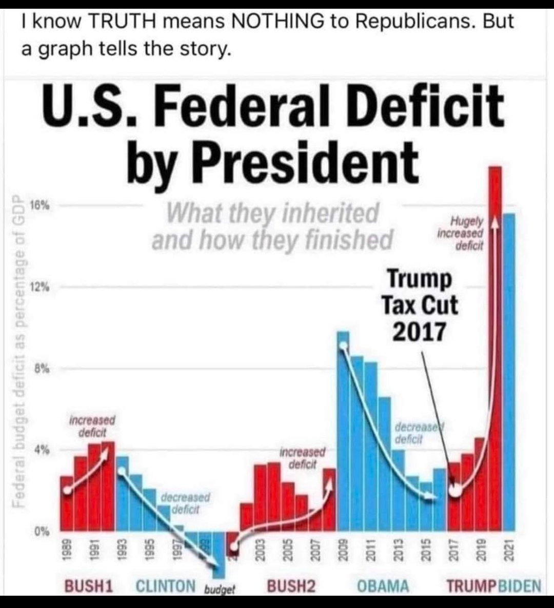
@SpeakerMcCarthy There's no debate Congress has got to approve paying for existing debt. Don't try to make this a Republican - Democrat thing, because it not!