Netherlands' BESI: Samsung's Hybrid Bonding Adoption Decision Coming Soon
Samsung Electronics is expected to introduce hybrid bonding technology — projected to be at the heart of next-generation semiconductor production — around the middle of this year.
Dutch back-end equipment company BE Semiconductor Industries (BESI) stated during its Q1 earnings conference call on April 23 that "we should see more definitive news around the middle of this year regarding Samsung Electronics' (hybrid bonder adoption)." This is largely consistent with the outlook shared during the Q4/full-year 2025 earnings call in February, which indicated Samsung would adopt hybrid bonding in Q2.
Unlike conventional thermo-compression (TC) bonding, hybrid bonding does not use fine metal bumps to connect stacked semiconductor dies. Instead, it is an advanced packaging technology that directly connects the copper (Cu) surfaces of two chips. When applied to High Bandwidth Memory (HBM) and new high-layer-count NAND flash, it can deliver performance improvements, reduced power consumption, and cost savings — because the direct copper-to-copper connection enables higher integration density and shorter interconnect lengths.
That said, some observers suggest that hybrid bonding adoption could be delayed as the Joint Electron Device Engineering Council (JEDEC) moves to relax packaging height limits for next-generation HBM. On this point, BESI CEO Richard Blickman explained, "The only reason (JEDEC) is looking to relax HBM thickness specifications is because one of the three memory companies needs that height for its process," adding that "the other two are not affected by this change." The major HBM players are Samsung Electronics, SK Hynix, and Micron. The implication is that two of these three are pursuing hybrid bonding adoption for reasons beyond height considerations.
Hybrid bonding produces chip-to-chip gaps of around 7 micrometers (㎛), which makes it advantageous for reducing the total thickness (height) of HBM packages. JEDEC is reportedly considering raising the height limit from the current 775㎛ to either 825㎛ or 900㎛. Analysts argue that if the package height limit is relaxed, the lifespan of existing TC bonding technology would be extended, while the introduction of hybrid bonding could be delayed — since hybrid bonding would no longer be required simply to reduce thickness.
Blickman emphasized, "The advantages of hybrid bonding over conventional TC bonding — faster circuit speeds, lower power consumption, and reduced heat — are being increasingly clearly demonstrated," and "as Samsung Electronics has publicly disclosed, because of these technical benefits, (the relaxation of HBM thickness limits) has not changed the pace or rate of hybrid bonding adoption."
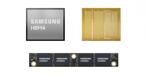
Samsung Electronics introduced its hybrid bonding technology for HBM at NVIDIA's annual developer conference, GTC 2026, last March. At the time, Samsung stated that hybrid bonding improves thermal resistance by more than 20% versus TC bonding and supports 16-high and higher stacks. Interconnect density is also higher. According to BESI, hybrid copper bonding (HCB) offers 15× the interconnect density of TC bonding and more than 100× the energy-efficiency performance (EEP).
BESI expects mass production of hybrid-bonding-based HBM to begin next year. Blickman explained, "All three manufacturers are conducting equipment evaluations against the same criteria set by a specific end customer," and "that end customer has asked the memory makers to secure hybrid-bonded stacked products by the end of this year, with the goal of bringing finished products to market next year." The end customer in question is most likely NVIDIA.
BESI is regarded as the global leader in the hybrid bonding equipment market. It holds a technological edge in both precision and throughput, particularly in die bonding equipment. Applied Materials, the world's largest semiconductor equipment company, holds a 9% stake, making it BESI's largest shareholder.