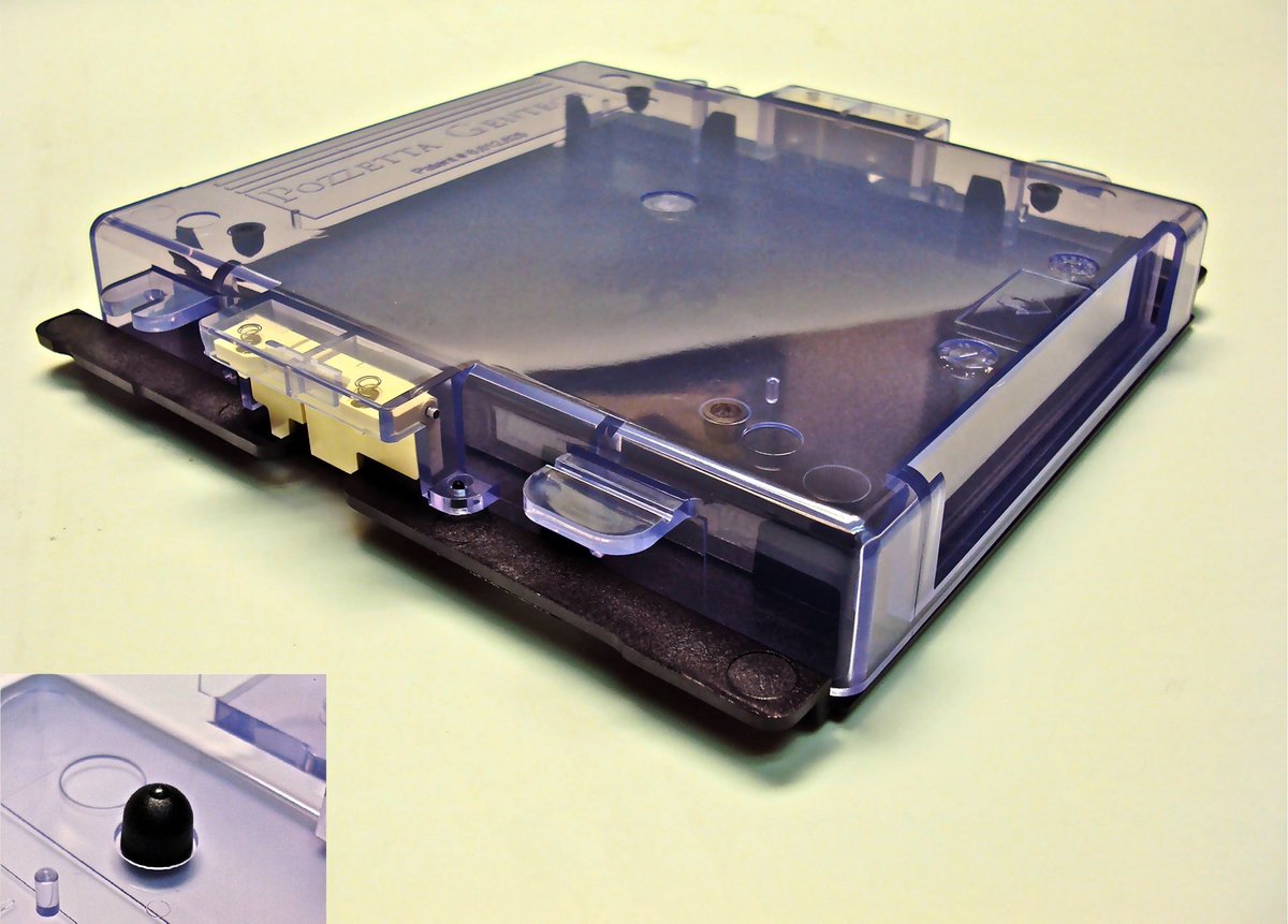
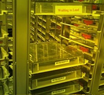
Proper organization helps protect valuable photomasks, improve accessibility, and keep cleanroom workspaces organized. Syntec designs custom reticle and photomask storage racks built around the needs of semiconductor fabs. #Semiconductor#ReticleStorage#Photomasks
Building the semiconductor workforce takes collaboration across the entire ecosystem.
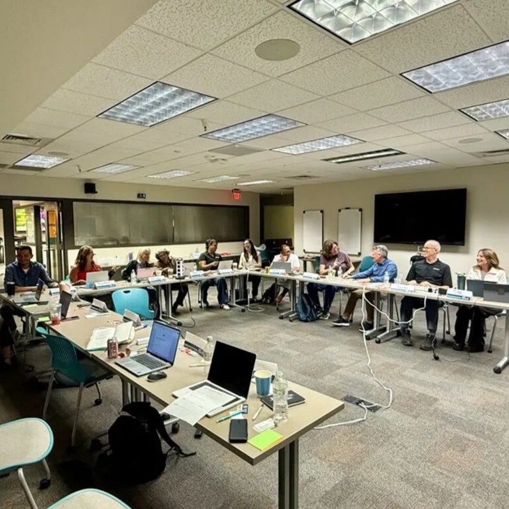
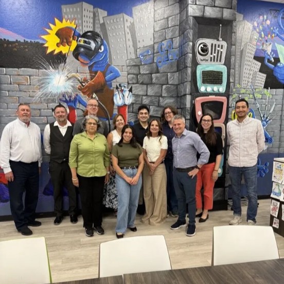
Recently, the @semifoundation convened experts from Advantest, @AmkorTechnology, @EMD_Electronics, FM Industries, @Intel and TSMC, alongside educators and workforce development leaders, at GateWay Community College in Phoenix, to help define micro-credentials for semiconductor manufacturing.
Over three days, participants identified key competencies, prioritized areas for assessment, and developed test questions focused on the practical knowledge of today's semiconductor workforce needs.
The group recommended four focus areas for new and upcoming micro-credentials:
• Cleanroom operations and safety
• Fab maintenance, tools, and metrology
• Vacuum technology
• Gas and chemical distribution systems
Brent Weil, president of Strategic Workforce Partners, and Anissa Hamden Morison, Curriculum Developer and Training Manager for the SEMI Foundation, share an update of the meeting and how you can get involved in supporting the workforce of tomorrow: https://t.co/LiCSWYCWak
#SEMI #Semiconductors #WorkforceDevelopment
Halloween is full of surprises. Your #tech should be ready for them. 👻
Memory and storage help technology process data at the edge and turn it into intelligence in real time.
Here’s to quick reactions and #Halloween fun. 🎃
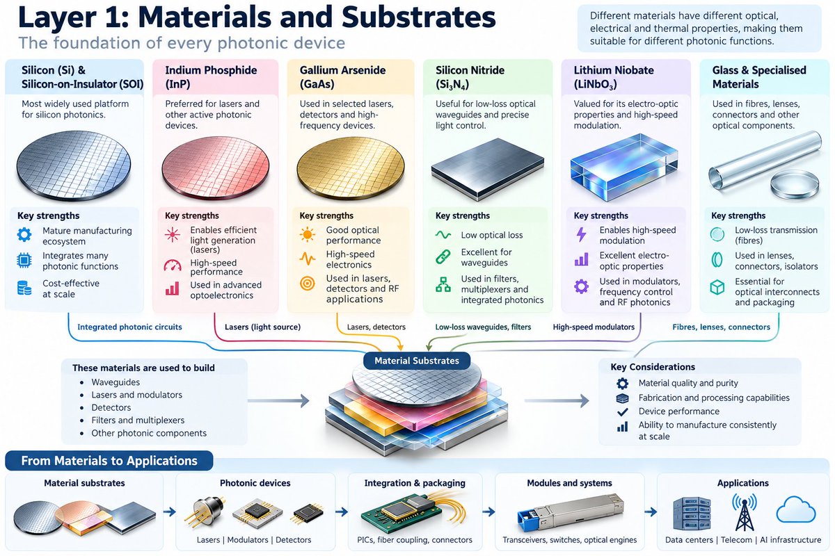
Photonics: The materials behind the next computing revolution
👉 Before light can carry data, it needs the right materials. Different substrates perform different functions across the photonics value chain:
→ Silicon & SOI: Integrated photonic circuits
→ Indium Phosphide (InP): Lasers and active photonic devices
→ Gallium Arsenide (GaAs): Selected lasers and high-frequency devices
→ Silicon Nitride (Si₃N₄): Low-loss waveguides and filters
→ Lithium Niobate: High-speed optical modulation
→ Specialised glass: Optical fibres, lenses and connectors
👉 The photonics opportunity extends beyond chips to material purity, substrate manufacturing, fabrication, packaging, optical testing and integration.
👉 As AI data centres demand faster, higher-bandwidth connectivity, these materials become critical building blocks for optical engines, transceivers and integrated photonic systems.
👉 India’s opportunity lies in building capabilities across this specialised materials and manufacturing ecosystem.
Breaking News: A Chinese businesswoman who had a close relationship with Nvidia’s CEO, Jensen Huang, was found to be passing intelligence to Beijing. https://t.co/0WLYYhR47a
As Infineon advances 300mm semiconductor manufacturing, proper wafer storage becomes increasingly important. Syntec USA provides industrial-grade stainless steel storage racks designed to support cleanroom organization, wafer protection, and efficient fab operations. #ai