Stop chasing EMC issues with shields and ferrites after the fact. 🔧
Most EMC problems are baked into the PCB long before the first test.
When failures happen, teams often reach for:
• Shielding
• Ferrite beads
• Extra filters
But in reality, the damage is already done—by placement, routing, return paths, and loop areas.
A board doesn’t fail EMC because the schematic is wrong.
It fails because the PCB layout let noise spread.
🟡 EMC starts inside your board
Before you even think about external emissions, your board has:
• Switching power loops
• High-speed clocks
• Noisy power traces
• Sensitive analog or low-level signals
If those are placed or routed carelessly, your board fights itself before testing ever begins.
🟡 Find the real noise source first
Most EMC issues come from:
• High dv/dt nodes → electric-field coupling
• High di/dt loops → magnetic-field coupling
Start with DC/DC switching nodes, clocks, and fast current loops. That’s where the trouble usually lives.
🟡 Loop area is a silent killer
For Buck, Boost, SEPIC, and other switching converters, the high-frequency current loop is critical.
Large loop = more radiation + stronger coupling + weaker filters.
Small loop = quieter board.
🟡 Partitioning is your first filter
Separate early:
• Digital vs. analog
• Noisy vs. sensitive
• Power vs. signal
• High frequency vs. low frequency
Good partitioning stops coupling before it starts.
🟡 Ground is a return path, not just a reference
Many EMC problems are actually return path problems.
If ground is fragmented or poorly shared:
• Loop area grows
• Impedance rises
• Noise coupling increases
A continuous, well-controlled return path solves more than you’d think.
🟡 Power routing is a major EMC decision
Power is both a noise source and a victim.
Good power layout means:
• Decoupling caps close to pins
• Power path close to return path
• Noisy loops kept local
• Unrelated power domains separated when needed
Many “EMC fixes” are just corrections to poor power routing.
🟡 Clock routing needs extra discipline
Clocks are tricky—they’re both sensitive and strong interferers.
Short crystal connections, tight local return paths, and clean placement matter more than most engineers expect.
📌 Bottom line
EMC problems aren’t created during testing.
They’re created during layout.
Control the:
• Noise source
• Coupling path
• Loop area
• Return path
Good EMC design isn’t about adding more parts.
It’s about letting your board coexist peacefully from the start.
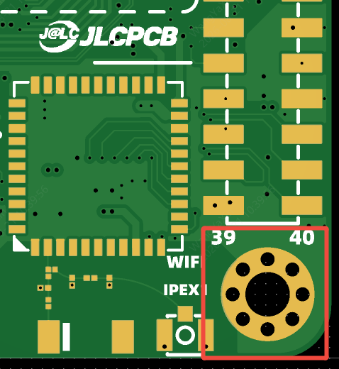
The vias around PCB mounting holes aren’t just decoration.
A via ring around a grounded mounting hole can:
✅ Improve connections to internal ground planes
✅ Help reinforce the surrounding copper
✅ Provide some local heat spreading
✅ Add redundant grounding paths
1 SAATLİK KURS İLE SIFIRDAN OYUN YAP
Stanford üniversitesinde Claude kod ajanları kullanarak 1 saat gibi kısa sürede kendi oyununu yaratmanı göstermişler.
Kimseye ihtiyacın yok bir laptop ,claude ve bu eğitim
Türkçe altyazı da benden
iyi seyirler.
Así se ve un sueldo de 750.000 dólares al año: un tipo en camiseta blanca, un pizarrón y 2 horas y media.
Stanford, CS336. Percy Liang construye un LLM desde cero. Lo que hay debajo de Claude y ChatGPT, y arranca por la parte que todos saltan: el modelo no lee tu texto, lee números.
Anthropic paga ese sueldo a los ingenieros que entienden esa capa.
Lo único que cobra Stanford son 2 horas y media de tu atención.