saat paling menyakitkan sekaligus menyedihkan adalah saat tidak lagi mengakui eksistensi diri sendiri.
semuanya terlihat hampa,seperti angin yang berlalu lalang begitu saja.
Google has published a paper that might end the transformer era.
For the last 7 years, every major AI, ChatGPT, Claude, Gemini, has been built on the exact same architecture: The Transformer.
But Transformers have a fatal flaw.
To remember context, they have to process every single word against every other word. It’s called quadratic complexity. As your prompt gets longer, the compute cost explodes.
The alternative is the old-school RNN (Recurrent Neural Network). RNNs are incredibly cheap and fast, but they have a fixed memory size. If you give them a long document, they get amnesia.
Until today.
Google researchers published Memory Caching: RNNs with Growing Memory.
And it fixes the biggest bottleneck in AI.
Instead of an RNN having a fixed, rigid memory that constantly overwrites itself, Google gave it a "save" button.
The technique allows the RNN to cache checkpoints of its hidden states as it reads.
The memory capacity of the RNN can now dynamically grow as the sequence gets longer.
They built four different variants, including sparse selective mechanisms where the AI actively chooses exactly which checkpoints matter most.
The results rewrite the rules of efficiency.
On long-context understanding and recall-intensive tasks, these new Memory-Cached RNNs closed the gap with Transformers.
They achieved competitive accuracy without the explosive, quadratic compute cost. It perfectly bridges the gap between the cheap efficiency of an RNN and the massive capability of a Transformer.
We have spent billions scaling Transformers because we thought they were the only way an AI could remember a long conversation.
But Google just proved we don't need to process the whole history every single time.
We just needed a smarter cache.
I met my younger self for Coffee today.
I lit a cigarette, He left the table.
I spoke of money, He spoke of dreams.
I showed him my watch, He showed me his sketches.
I laughed at his innocence, He cried for my soul.
We sat in silence, two strangers in the same skin.
-Stephen Okpelle
Every modern OLED or microLED display is built on nanometer scale thin films whose uniformity determines whether a panel becomes functional or scrap. Across glass substrates reaching 1500 × 1850 mm Gen 6 class sizes, billions of pixels depend on organic or inorganic layers controlled at thickness scales typically in the 5–50 nm regime per emissive stack, where even minor deviation shifts color accuracy, efficiency, and lifetime.
The core constraint is vacuum thin film deposition stability. OLED layers are formed in ultra high vacuum environments operating around 10⁻⁶ to 10⁻⁷ torr class pressure regimes, where organic materials are thermally evaporated or deposited in tightly controlled flux conditions. Any instability in evaporation rate or chamber pressure directly translates into nanometer level thickness variation, which propagates into brightness non uniformity across the panel.
At the pixel level, yield becomes a probabilistic system where single particle contamination at sub micron scale can deactivate multiple pixels simultaneously, making defect density the dominant economic variable in manufacturing. This creates a nonlinear yield collapse behavior where small increases in contamination frequency can disproportionately reduce usable panel output across large substrates.
MicroLED systems shift the bottleneck from deposition to transfer and alignment, where millions of microscopic inorganic emitters must be positioned with micron to sub micron precision. Each alignment error translates into missing pixels or brightness inconsistency, forcing complex mass transfer and repair systems to recover yield.
Material systems such as indium tin oxide and gallium nitride require electronics grade purity at PPM to PPB levels, where trace contamination alters conductivity, recombination efficiency, and emission stability. This couples chemical purity directly into optical output behavior.
Global production is concentrated across Samsung Display, LG Display, and BOE, where the key advantage is not material access but repeatable nanometer scale uniformity across industrial scale substrates.
Display manufacturing therefore functions as a constrained thin film physics system where vacuum stability, nanometer deposition control, and defect suppression determine whether billions of pixels can reliably emit uniform light across meter scale surfaces.
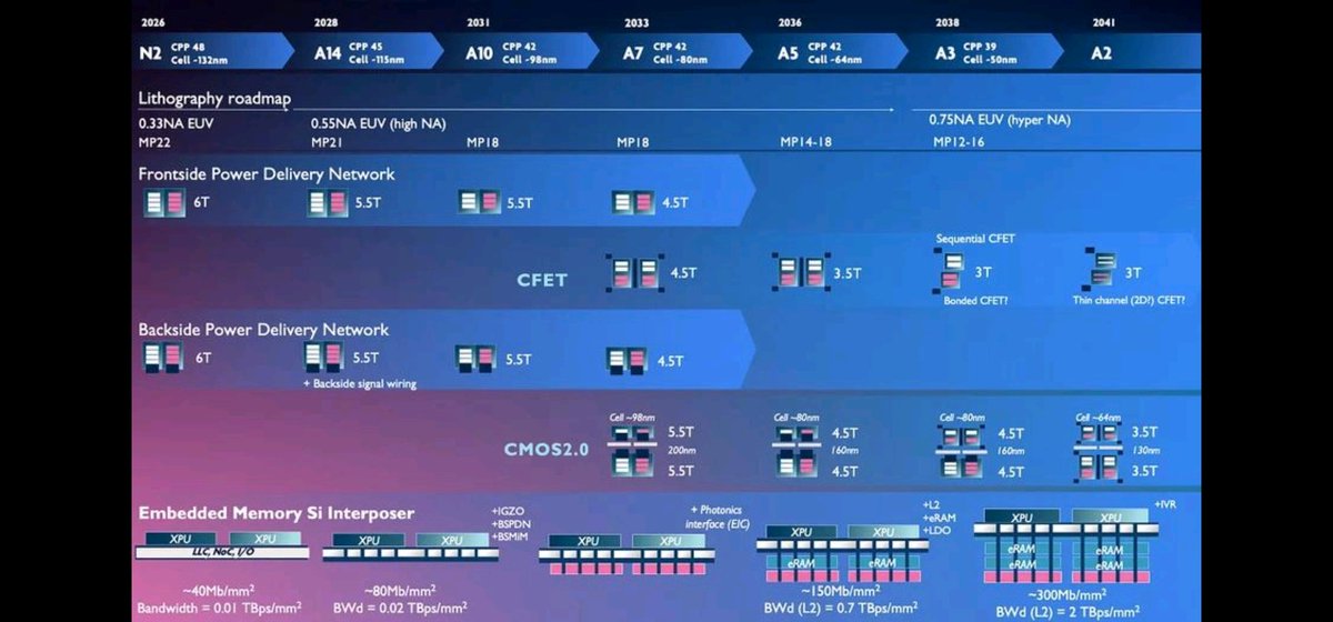
IMEC 2026–2041 Semiconductor Roadmap
Timeline: Nodes advance from N2 (2026) through A14 (2028), A10 (2031), A7 (2033), A5 (2036), A3 (2038) to A2 (2041).
Lithography: Progresses from 0.33 NA EUV (2026) to 0.55 NA High-NA (2028) and 0.75 NA Hyper-NA (2038)
CPP Scaling: Contacted Poly Pitch shrinks from 48 nm to 39 nm, enabling continued density gains.
Transistor Architecture: Standard cells reduce from 6T → 3T; major shift to CFET, Bonded CFET, and thin-channel (2D) CFET for improved performance and power efficiency.
Power Delivery: Frontside and backside networks converge on 3T–3.5T cells with backside signal routing, significantly lowering power consumption and routing congestion.
Embedded Memory: Density rises from ~40 Mb/mm² to ~300 Mb/mm²; bandwidth increases from 0.01 TBps/mm² to 2 TBps/mm² via silicon interposers, eRAM, photonics, and integrated voltage regulation.
Хуавей с чипом Кирин 9050 по факту заявил о достижении 2-3 нм техпроцесса в Китае:
«238 млн. транзисторов на 1 кв. мм»
DUV литограф с ArF-лазером 193 нм даёт 90 нм
+ иммерсия в оптике — до 45 нм
+ мультимаски и 3д-транзисторы — до 10 нм
+ стекирование кристалла по «Тау» — 2 нм?
@heartylene Hmmm dlu pernah pengalaman transaksi sama temen di Malaysia pake qris via dana, g pake pajak ato apa, lgsg convert ke Ringgit di dananya ga pake ribet
AMD's Zen. Apple's A4. Tesla's Autopilot chip.
Three industries. Three revolutions. One man designed them all. 🤯
Meet Jim Keller 🇺🇸
> Born in New Jersey. Penn State engineering grad.
> Started at Digital Equipment in 1982 ~ designed Alpha processors for 15 years
> Joined AMD in 1998. Designed the K7 and K8 chips.
> AMD beat Intel for the first time ever.
> Co-wrote x86-64 ~ the instruction set running every modern PC and server on earth
> Moved to Apple in 2008. Led the A4 and A5.
> The brain inside iPhone 4 and 4S.
> Returned to AMD in 2012. Stock was around $2. Company was dying.
> Designed Zen from zero.
> He left before Ryzen even launched.
> AMD went from $2 to a $250B company anyway. 🚀
> Joined Tesla in 2016. Built the Full Self-Driving chip.
> Joined Intel in 2018 to fix their CPU collapse.
> Now CEO of Tenstorrent ~ taking on Nvidia in AI chips.
> AMD's former CTO calls him "The Forrest Gump of chip design"
The most important engineer you've never heard of.
Absolute Legend 🐐